Hydrogen-plasma process for surface preparation prior to insulator deposition on compound semiconductor materials

a semiconductor material and surface preparation technology, applied in the field of semiconductor materials, can solve the problems of lack of reproducibility and high defect of native oxides, and achieve the effects of reducing the probability of contamination or reoxidation of the surface, excellent charge modulation, and reducing the frequency dispersion of accumulation capacitan

Inactive Publication Date: 2014-09-18
THE UNITED STATES OF AMERICA AS REPRESENTED BY THE SECRETARY OF THE NAVY
View PDF4 Cites 2 Cited by
  • Summary
  • Abstract
  • Description
  • Claims
  • Application Information

AI Technical Summary

Benefits of technology

[0014]One advantage of this surface oxide removal and modification technique is that all pre-treatment is done in situ, immediately prior to dielectric deposition, reducing the likelihood of contamination or reoxidation of surface possible with ex situ methods. Furthermore, highly defective native oxides are removed via clean and controlled indirect hydrogen plasma treatment. This hydrogen-plasma pretreatment approach avoids wet-chemical etches, which are subject to incidental contamination and lack of reproducibility. Additionally, MOS capacitors fabricated exhibit excellent charge modulation and decreased frequency dispersion of accumulation capacitance, indicating a reduction in undesired states at the dielectric / semiconductor boundary and an improvement in the electrical interface. Reduction in interface trap states on GaSb surfaces achieved with hydrogen plasma treatment are comparable, if not better than, other approaches. Moreover, comparable results can be achieved by tuning any one of multiple plasma parameters (power, exposure time, substrate temperature), allowing greater flexibility to accommodate substrate or instrumentation constraints.

Problems solved by technology

Furthermore, highly defective native oxides are removed via clean and controlled indirect hydrogen plasma treatment.
This hydrogen-plasma pretreatment approach avoids wet-chemical etches, which are subject to incidental contamination and lack of reproducibility.

Method used


Image

  • Hydrogen-plasma process for surface preparation prior to insulator deposition on compound semiconductor materials
  • Hydrogen-plasma process for surface preparation prior to insulator deposition on compound semiconductor materials

Examples


Embodiment Construction

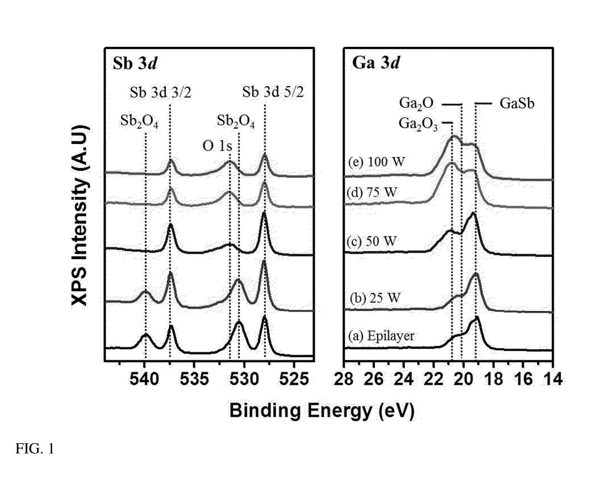
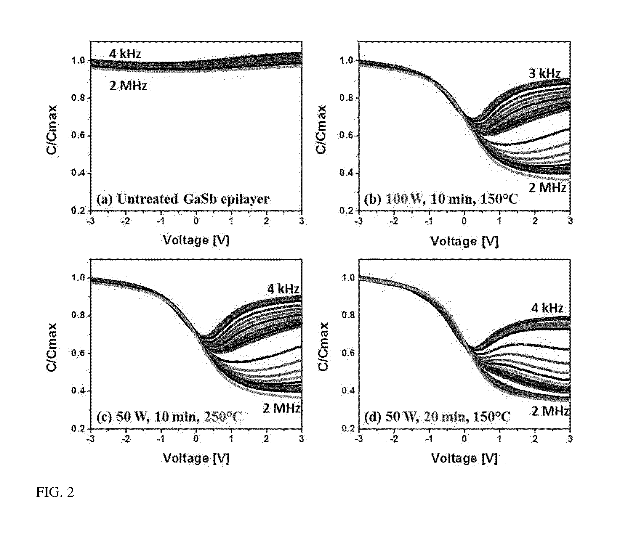
[0018]In the present invention, semiconductor substrates are loaded into an atomic layer deposition (ALD) reactor. The samples are exposed to a hydrogen plasma that acts to remove and / or modify any native oxide present on the surface. The effectiveness of the removal and modification of the native oxide layer can be tuned by varying the substrate temperature, hydrogen plasma power, and / or hydrogen plasma exposure time. Following plasma exposure, high-k dielectric deposition is accomplished via a standard ALD process without breaking vacuum and without exposing the sample to the atmosphere.

[0019]Semiconductor substrates are loaded into an atomic layer deposition (ALD) vacuum system equipped with a hydrogen plasma source. Once under vacuum, substrates are heated to the desired processing temperature, typically 150° C. to 300° C., which is less than the native oxide desorption temperature. After the base substrate temperature is reached, the samples are exposed to a hydrogen plasma tha...


PUM

PropertyMeasurementUnit
temperatureaaaaaaaaaa
hydrogen plasma poweraaaaaaaaaa

Abstract

A method of making a semiconductor material by pretreating a semiconductor substrate having a native oxide on the substrate surface under vacuum with hydrogen plasma to remove and/or modify the native oxide. After plasma exposure, a high-k dielectric is deposited in-situ onto the substrate using atomic layer deposition. There is no break in the vacuum between the plasma exposure and the atomic layer deposition. Also disclosed is the related semiconductor/dielectric material stack.

Description

PRIORITY CLAIM[0001]The present application is a non-provisional application claiming the benefit of U.S. Provisional Application No. 61 / 778,561, filed on Mar. 13, 2013 by Sharka M. Prokes et al., entitled “Hydrogen-Plasma Process for Surface Preparation Prior to Insulator Deposition on Compound Semiconductor Materials,” the entire contents of which is incorporated herein by reference.BACKGROUND OF THE INVENTION[0002]1. Field of the Invention[0003]The present invention relates generally to semiconductor materials and, more specifically, to hydrogen plasma pre-treatment of semiconductor materials.[0004]2. Description of the Prior Art[0005]Currently, many analog and nearly all digital electronics are fabricated from silicon-based materials. However, due to their superior electronic properties, compound semiconductors, such as GaSb, show promise as alternative materials for high-speed, high-performance electronic devices. In addition, the III-V compound semiconductors generally have di...

Claims


Application Information

Patent Timeline
Patent Type & Authority Applications(United States)
IPC IPC(8): H01L21/02
CPCH01L21/0226H01L21/02315C23C16/0245C23C16/45525
Inventor PROKES, SHARKA M.CLEVELAND, ERINRUPPALT, LAURA
Owner THE UNITED STATES OF AMERICA AS REPRESENTED BY THE SECRETARY OF THE NAVY
Why Eureka
Try Eureka