Photovoltaic Device Including A Back Contact And Method Of Manufacturing
a back contact and photovoltaic technology, applied in the field of photovoltaic devices, can solve the problems of device operation, loss, negative impact, etc., and achieve the effect of reducing the number of back contact layers
- Summary
- Abstract
- Description
- Claims
- Application Information
AI Technical Summary
Benefits of technology
Problems solved by technology
Method used
Image

Examples
first embodiment
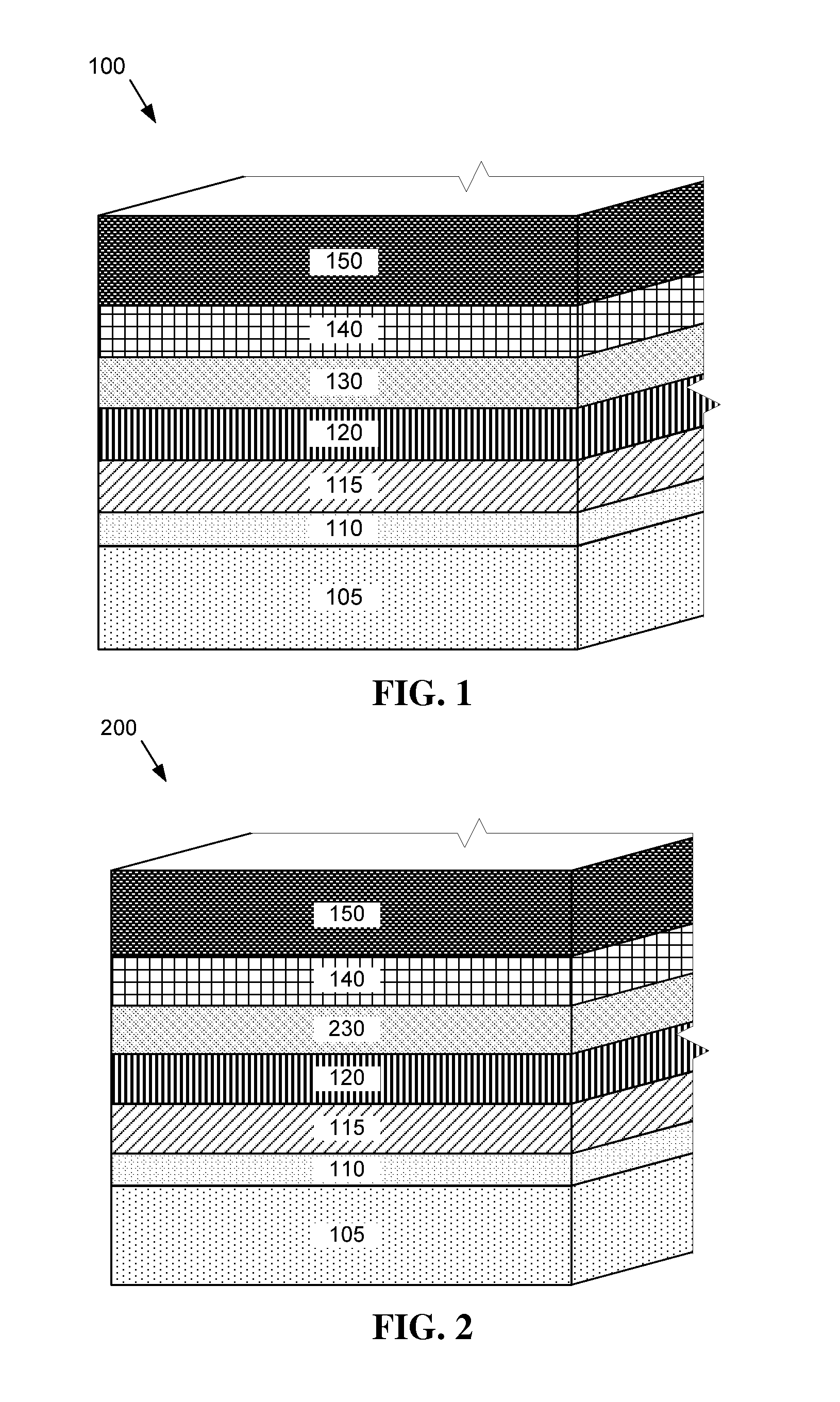
[0032] shown in FIG. 1, an electron reflector layer 130 is provided between the absorber layer 120 and the back electrode layer 140. In this embodiment, the electron reflector layer 130 is a zinc telluride (ZnTe) layer doped with copper telluride (Cu2Te).
[0033]Doping is a process of intentionally introducing impurities into an otherwise extremely pure material, such as a semiconductor material, in order to modulate its electrical or optical properties. In this embodiment, the electron reflector layer 130 contains primarily ZnTe with a Cu2Te dopant present in concentrations up to 5 at %. The compositional ratio (at %) of a compound, for example ZnTe:Cu2Te is determined by comparing the number of Cu2Te atoms in a given amount of the material with the total sum of ZnTe atoms and Cu2Te atoms in the same given amount. For example, where x=5 at %, there are 19 ZnTe atom for every 1 Cu2Te atom in a given amount of ZnTe:(Cu2Te)5% material. The electron reflector layer 130 may be between abo...
second embodiment
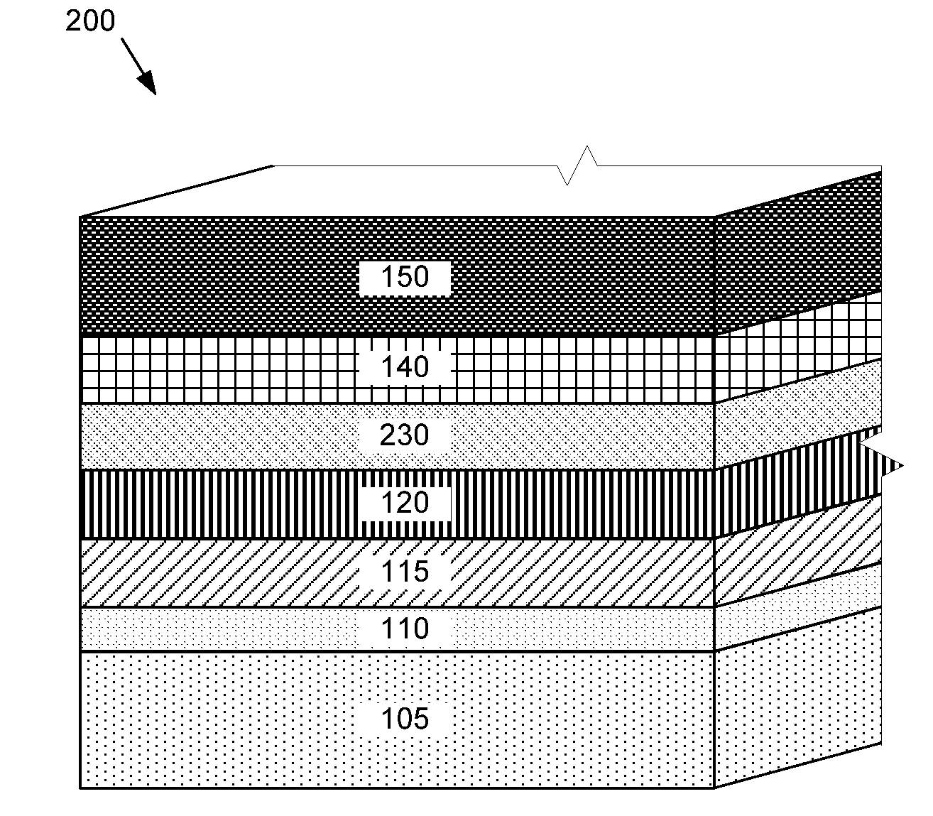
[0039]Referring now to FIG. 2, a second embodiment is shown where like layers are designated as in the prior embodiment and described above. A photovoltaic device 200 according to the present embodiment includes a window layer 115 deposited over a substrate structure including a base layer 105 and a TCO layer 110. An absorber layer 120 is deposited over the window layer 115. The window layer 115 and the absorber layer 120 form a p-n junction in the photovoltaic device 200. An electron reflector layer 230 is deposited over the absorber layer 120. A back electrode layer 140 and a back contact layer 150 are formed over the electron reflector layer 230.
[0040]The electron reflector layer 230 according to the present embodiment is provided between the absorber layer 120 and the back electrode layer 140. In this embodiment, the electron reflector layer 230 is a ZnTe / Cu2Te alloy. The electron reflector layer 230 may be between about 5 nm to about 25 nm thick or alternatively between about 1...
third embodiment
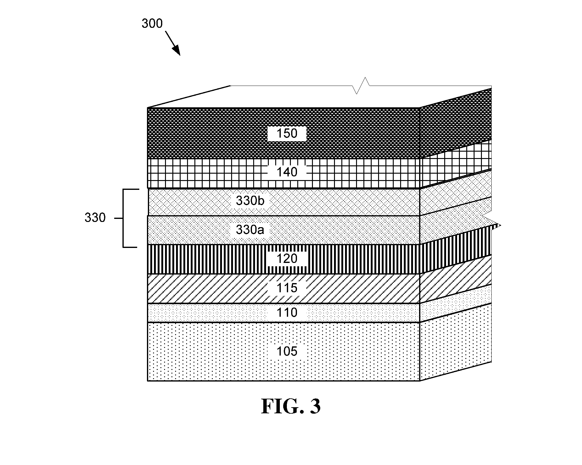
[0047]Referring now to FIG. 3, a photovoltaic device 300 is shown where like layers are designated as in the prior embodiments and described above. A photovoltaic device 300 according to the present embodiment includes a window layer 115 deposited over a substrate structure including a base layer 105 and a TCO layer 110. An absorber layer 120 is deposited over the window layer 115. The window layer 115 and the absorber layer 120 form a p-n junction in the photovoltaic device 300. An electron reflector layer 330 is deposited over the absorber layer 120. A back electrode layer 140 and a back contact layer 150 are formed over the electron reflector layer 330.
[0048]The electron reflector layer 330 according to the present embodiment is provided between the p-type absorber layer 120 and the back electrode layer 140. In this embodiment, the electron reflector layer 330 includes multiple sublayers 330a and 330b. The electron reflector sublayer 330a adjacent to the absorber layer 120 may be...
PUM
 Abstract
Description
Claims
Application Information
 - R&D
- Intellectual Property
- Life Sciences
- Materials
- Tech Scout
- Unparalleled Data Quality
- Higher Quality Content
- 60% Fewer Hallucinations
Browse by: Latest US Patents, China's latest patents, Technical Efficacy Thesaurus, Application Domain, Technology Topic, Popular Technical Reports.
© 2025 PatSnap. All rights reserved.Legal|Privacy policy|Modern Slavery Act Transparency Statement|Sitemap|About US| Contact US: help@patsnap.com