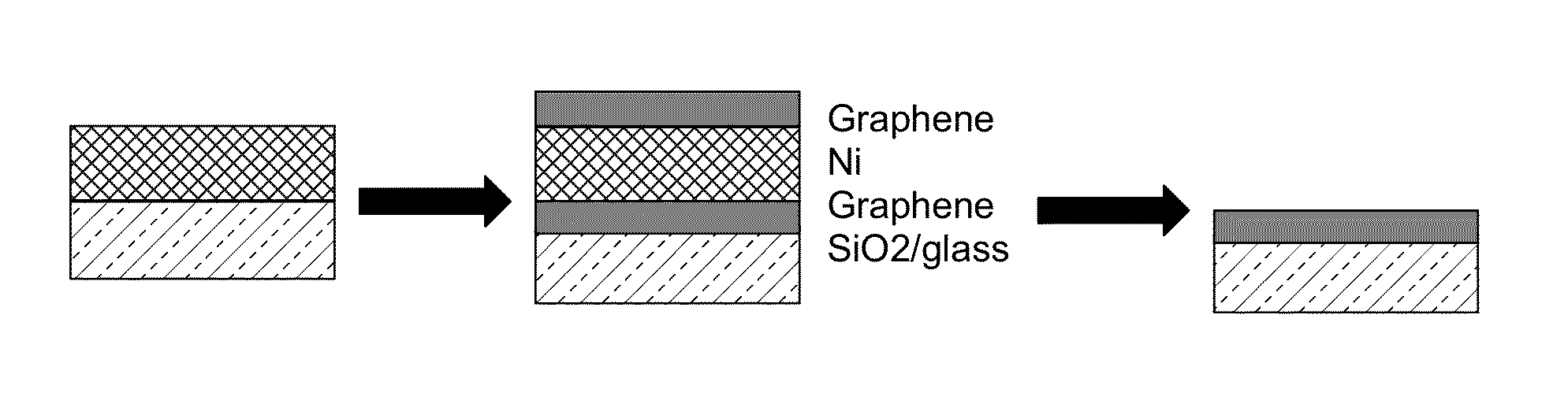
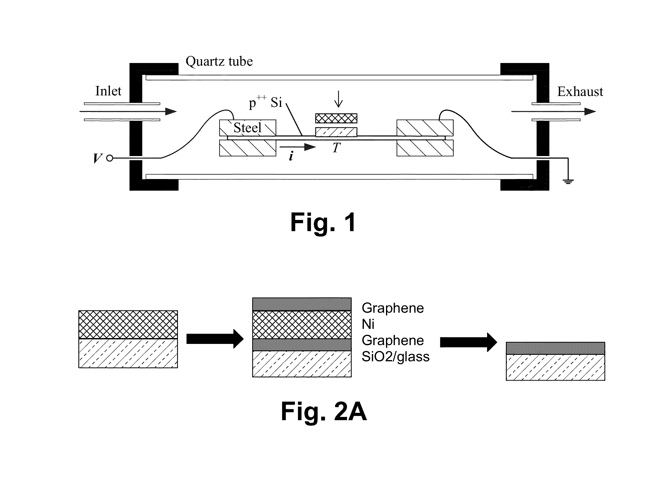
Methods for direct production of graphene on dielectric substrates, and associated articles/devices
a technology of dielectric substrates and graphene, which is applied in the direction of conductors, transportation and packaging, coatings, etc., can solve the problems of the inability to meet the requirements of the near infrared region
- Summary
- Abstract
- Description
- Claims
- Application Information
AI Technical Summary
Benefits of technology
Problems solved by technology
Method used
Image

Examples
case 3
sic Sources of Stress—Lattice Mismatch and Creep
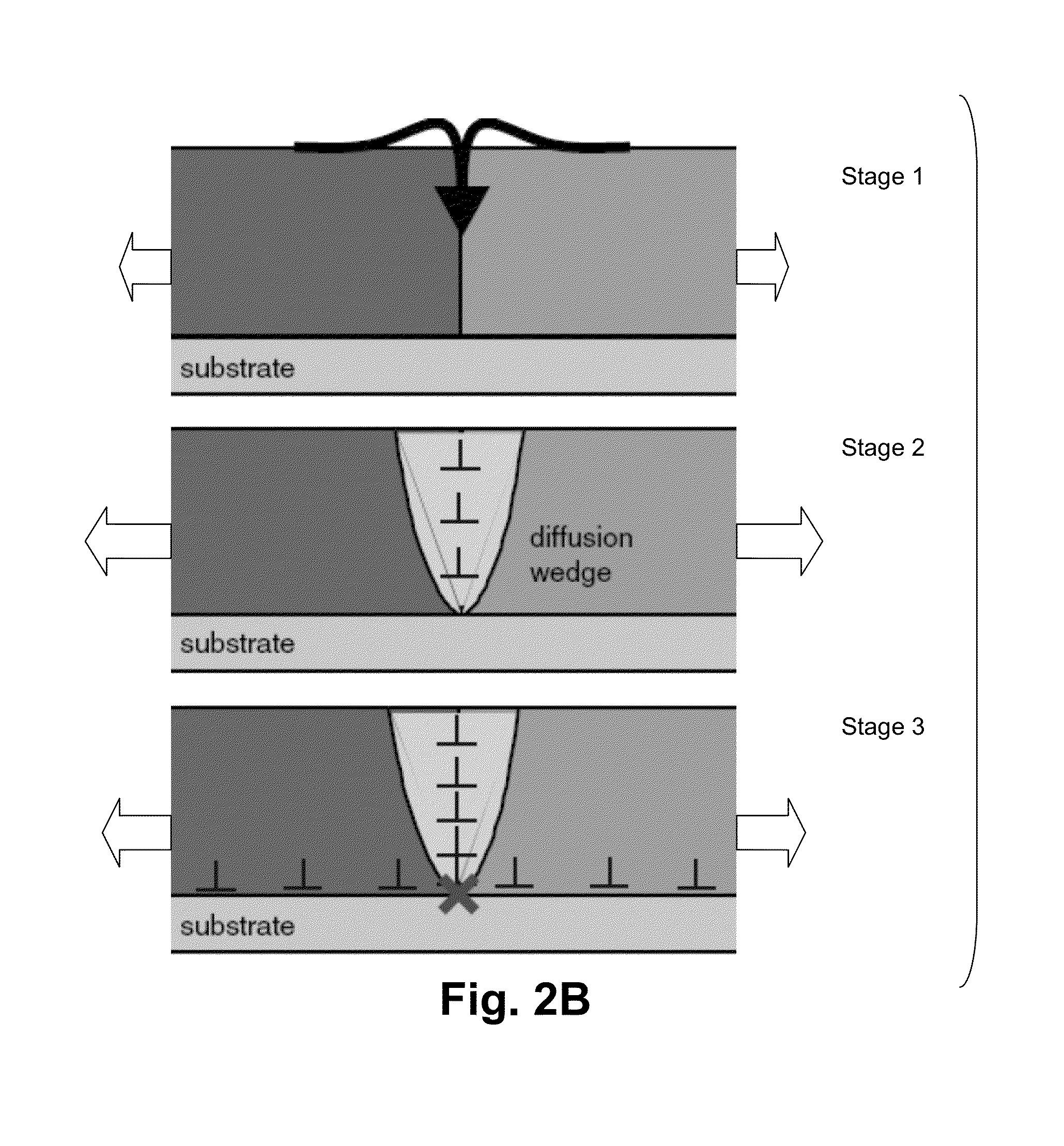
[0144]In the above model, the grain boundary “zipping up” does not happen at once. After the initial coalescence, the grain boundary formation may proceed layer by layer when it is energetically favorable. If the distance between two layers is too far, the layers may grow laterally during deposition until the attracting force is large enough to pull together. This mechanism produces less tensile stress than the traditional zipping up processes, which often overestimate the tensile stress.
example stress
-Induced Softening and Stiffening of Raman Modes at Fixed Growth Temperature
[0145]It is well known that softening of the Raman modes happens as temperature is increased. See FIG. 13, which plots biaxial stress against temperature for a sample made in accordance with certain example embodiments. It is proposed herein that the red-shift of the Graphene films due to temperature be baseline for a standard film grown in the reactor. This baseline can be used to track the red or blue shift due to stress changes.
An Example Continuum Interfacial Stress Model
Thermal Stress Evolution: Heat Ramp-Up
[0146]Tensile stress in the as-deposited nickel catalyst film may originate from excess volume. From the electron and XRD data, the films are amorphous in the thickness range of 100 nm to 1 micron. The constraint imposed by the strong bonding between film and substrate implies that neither sliding nor inter-diffusion can occur at the film / substrate interface. As the Ni film is thermally annealed, the...
case 1
[0172]Since carbon atoms in the solid solution is being replenished by constant supply from the feedstock hydrocarbon gas, one can make the reasonable assumption that competition for solute atoms between neighboring dislocations can be neglected. It therefore can be assumed that there is a constant replenishment of C at the interface. When flow due to the concentration gradient is ignored and the potential interaction φ has a purely radial form given by
Ψ(r)=-Ψ0r2(65)
[0173]then the pure drift solution is obtained from the first-order equation:
∂C∂t=DkTΨ0r3(∂C∂r-2Cr)(66)
[0174]The above equation can be solved to show that ratio of concentration of carbon atoms arriving at the dislocation in a time t to the initial concentration is given by:
C(t) / C0=πρ(6πrpΨ0DkTt)3 / 5(67)
PUM
| Property | Measurement | Unit |
|---|---|---|
| pressure | aaaaa | aaaaa |
| pressure | aaaaa | aaaaa |
| pressure | aaaaa | aaaaa |
Abstract
Description
Claims
Application Information