Fabrication method of a rigid-flexible circuit board and rigid-flexible printed circuit board

a technology of printed circuit board and fabrication method, which is applied in the direction of printed circuit manufacturing, printed circuit assembling, printed circuit aspects, etc., can solve the problems of increasing the virtually fabrication cost of electronic devices (or products) using such pcbs, the waste of flexible sheets of all electronic products, and the relatively high fabrication cost of fccls. achieve the effect of small expansion and contraction variation, small overlap area, and significant reduction of flexible sheet was

Inactive Publication Date: 2014-10-30
PEKING UNIV FOUNDER GRP CO LTD
View PDF3 Cites 20 Cited by
  • Summary
  • Abstract
  • Description
  • Claims
  • Application Information

AI Technical Summary

Benefits of technology

[0008]In view of the disadvantages that fabrication costs of rigid-flexible PCBs are high and fabrications are difficult in the prior art, the technical problems to be solved by the present invention are to provide a fabrication method of a rigid-flexible PCB with low fabrication cost, and to provide a rigid-flexible PCB fabricated by the fabrication method.
[0033]According to a fabrication method of the present invention, the flexible board unit is embedded in the rigid board, and a wiring pattern on the flexible board is connected with a wiring pattern on a layer in which the rigid board is located, such that when fabricating a rigid-flexible PCB, it is only necessary to provide the flexible window region in the rigid board and dispose the flexible board unit in the flexible window region accordingly, without using flexible sheet in an entirety layer in which the flexible region of the rigid-flexible PCB is located, thus significantly reducing waste of flexible sheets, and accordingly lowering fabrication cost of a rigid-flexible PCB; at the same time, in a rigid-flexible PCB fabricated by such fabrication method, as the flexible board and the rigid board have a relatively small overlapping area, expansion and contraction variations of the flexible sheet in the flexible board are substantially consistent with those of the rigid sheet in the rigid board, and when performing lamination, undesirable phenomena such as misalignment of patterns, dislocations and the like due to inconsistent expansion and contraction variations will not occur. When performing drilling, hole cleaning and hole metallization processes, as the rigid region is a completely rigid sheet, processing thereof can be performed in full accordance with machining process and machining parameters of a rigid board, thus testing and debugging are omitted; as to the flexible region, when fabricating a fine pattern, small size machining may be used because the flexible board unit has small expansion and contraction variations and is difficult to be damaged, and meanwhile, undesirable phenomena such as open circuit, short circuit and the like may be effectively prevented from occurring, degree of difficulty in fabricating a rigid-flexible PCB is thus lowered and quality of a rigid-flexible PCB is effectively improved.
[0034]In summary, the beneficial effects of the present inventions are: significantly lowering fabrication costs of rigid-flexible PCBs, improving production yield and reliability of PCBs, and particularly improving connection reliability of PCBs; lowering degree of difficulty in fabricating rigid-flexible PCBs, and being especially suitable for fabricating rigid-flexible PCBs with four or more than four layers.

Problems solved by technology

With continuous development of production technology, all electronic products tend to become light and small.
Meanwhile, fabrication costs of FCCLs are relatively high, which increases virtually fabrication costs of electronic devices (or products) using such PCBs.
Additionally, in order to reduce flow of prepreg in regions (i.e., rigid-flexible regions) where rigid regions and flexible regions overlap each other, low flow prepregs are generally used in fabricating rigid-flexible PCBs; while low flow prepregs are more expensive than ordinary prepregs, which directly increases costs of electronic devices (or products).
Estimation shows that fabrication cost of a rigid-flexible PCB is 5-7 times that of a standard FR-4 rigid board at present, high costs limit further applications and developments of rigid-flexible PCBs.
It can be seen that, in current fabrication methods of rigid-flexible PCBs, since both use of a mixture of various materials and processing of a multilayer board are involved, the fabrication cost is high and the fabrication is difficult, and generally, such method is only suitable for fabricating a rigid-flexible PCB with less than ten layers.

Method used


Image

  • Fabrication method of a rigid-flexible circuit board and rigid-flexible printed circuit board
  • Fabrication method of a rigid-flexible circuit board and rigid-flexible printed circuit board
  • Fabrication method of a rigid-flexible circuit board and rigid-flexible printed circuit board

Examples


embodiment 1

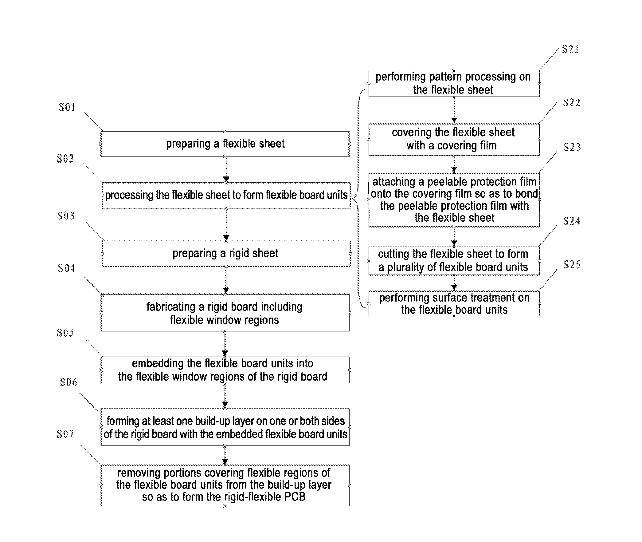
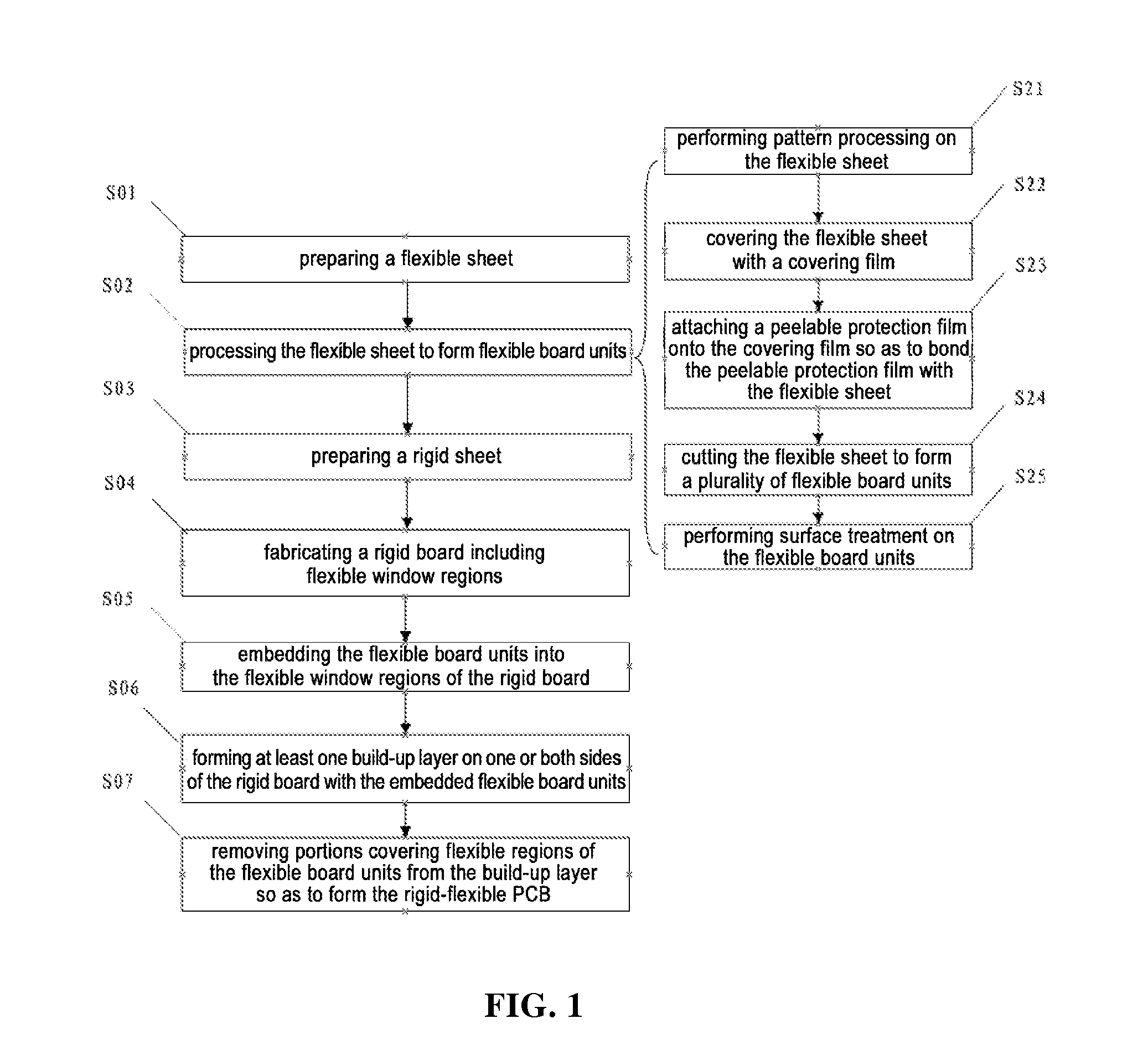
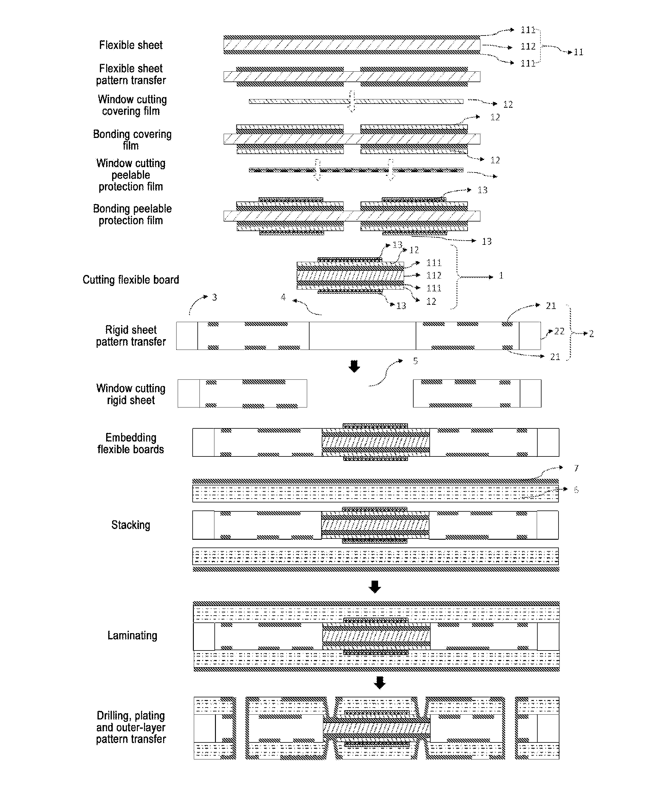
[0053]The circuit board fabricated in this embodiment is a Plus One HDI rigid-flexible PCB, and FIG. 2 is a diagram showing processing steps of fabricating the Plus one HDI rigid-flexible PCB. As illustrated in FIG. 1, the fabrication method specifically includes the following steps:

[0054]Step S01: preparing a flexible sheet. In this embodiment, the flexible sheet 11 includes a flexible sheet dielectric layer 112 and flexible sheet conductive layers 111 provided at both sides of the flexible sheet dielectric layer 112.

[0055]Step S02: processing the flexible sheet 11 to form small flexible board units. Each small flexible board unit is divided into a rigid-flexible region and a flexible region.

[0056]The step of processing the flexible sheet specifically includes:

[0057]Step S21: performing pattern processing on the flexible sheet. That is, transferring a wiring pattern that needs to be arranged in the flexible board onto the flexible sheet conductive layers 111 on both sides of the fl...

embodiment 2

[0079]A circuit board fabricated in this embodiment is a high plus (Plus two or higher) HDI rigid-flexible PCB. FIG. 3 is a diagram showing processing steps of fabricating the HDI rigid-flexible PCB. In this embodiment, the high plus HDI rigid-flexible PCB is a Plus N (N≧2) HDI rigid-flexible PCB. As illustrated in FIG. 3, the method specifically includes the following steps:

[0080]fabricating an inner-layer board. This step includes the same steps as steps S01-S06 in Embodiment 1, the obtained rigid board with embedded flexible board units is the inner-layer board of this embodiment.

[0081]Adding a required number of layers of rigid sheets after the above step S62, and this step specifically includes:

[0082]Step S63: stacking. A copper foil 7 is first placed, a prepreg 6 is placed on the copper foil 7, the obtained inner-layer board is then placed on the prepreg 6, and a prepreg 6 and a copper foil 7 are sequentially placed on the inner-layer board. Through the above stacking, the num...

embodiment 3

[0090]A circuit board fabricated in this embodiment is a Plus one HDI rigid-flexible PCB. As illustrated in FIG. 4, this embodiment differs from Embodiment 1 in that:

[0091]1) Corresponding to step S06 in Embodiment 1, in this embodiment, before stacking (S61), window cutting is first performed on the prepreg 6. Herein, the window regions cut in the prepreg correspond to the flexible regions of the flexible board units, and the borders of the window regions correspond to the common borders of the flexible regions and the rigid-flexible regions of the flexible board units. Size of the windows cut in the prepreg has the same length as that of the rigid-flexible regions, specifically, the length ranges from 0.5 mm to 3 mm, while the width of the window regions ranges from 0-500 μm, and the windows can be formed by mechanical milling or laser cutting or die cutting. FIG. 9 is a processing schematic diagram of performing window cutting and stacking on the prepreg in Embodiment 3 of the pr...


PUM

PropertyMeasurementUnit
widthaaaaaaaaaa
thicknessaaaaaaaaaa
thicknessaaaaaaaaaa

Abstract

A manufacturing method of an anode foil for an aluminum electrolytic capacitor is provided, which comprises a first step of forming a porous oxide film, i.e. subjecting an etched foil having etched holes thereon to an anodic oxidation process to form a porous oxide film on both the outer surface of the etched foil and the inner surface of etched holes, and a second step of forming a dense oxide film, i.e. converting the porous oxide film into the dense oxide film. The method can be used to manufacture an anode foil for various voltage ranges, e.g. an ultra-high voltage anode foil whose voltage is more than 800 vf, and the method can increase specific capacity, reduce power consumption, simplify the process, and increase production efficiency.

Description

CROSS-REFERENCE TO RELATED APPLICATIONS[0001]The present application claims priority to International Application No. PCT / CN2012 / 081935 which was filed on Sep. 25, 2012 and claims priority to Chinese Patent Application No. 201110369904.8 filed Nov. 18, 2011.STATEMENT RE: FEDERALLY SPONSORED RESEARCH / DEVELOPMENT[0002]Not ApplicableFIELD OF THE INVENTION[0003]The present invention relates to the field of printed circuit board (PCB) technology, and particularly, to a fabrication method of a rigid-flexible PCB and a rigid-flexible PCB fabricated by the fabrication method.BACKGROUND OF THE INVENTION[0004]With continuous development of production technology, all electronic products tend to become light and small. Various mini-portable electronic products such as mobile phones, digital cameras and the like are results under development of High Density Interconnect (HDI) technology. HDI is a technique in which circuit board layers can be connected to each other through forming microchannels...

Claims


Application Information

Patent Timeline
Patent Type & Authority Applications(United States)
IPC IPC(8): H05K3/46H05K1/02
CPCH05K3/46H05K2203/061H05K1/02H05K3/4691H05K3/4694H05K2201/09127Y10T29/49126
Inventor HUANG, YONGCHEN, ZHENGQING
Owner PEKING UNIV FOUNDER GRP CO LTD
Why Eureka
Try Eureka