Broadband optical isolator using phase modulators and mach-zehnder interferometers

a phase modulator and optical isolator technology, applied in the field of optical isolators, can solve the problems of high manufacturing complexity, inability to manufacture magneto-optic materials using large-scale integrated circuit production techniques, and difficulty in integrating into chip-scale planar photonic circuits, so as to reduce the insertion loss and the achievable footprint, the effect of high operation frequency

Inactive Publication Date: 2014-11-13
NOKIA SOLUTIONS & NETWORKS OY
View PDF3 Cites 21 Cited by
  • Summary
  • Abstract
  • Description
  • Claims
  • Application Information

AI Technical Summary

Benefits of technology

[0008]Aspects of the present invention include a new non-reciprocal photonic circuit operating with standard single-mode waveguides in planar lightwave circuits, or in optical fiber systems. Embodiments of the invention may exploit time-dependent index modulation obtained with conventional phase modulators such as the one widely available in integrated photonics platforms. Because it is based on fully balanced interferometers and does not involve resonant structures, the scheme is also intrinsically broadband (>100 nm). Using realistic parameters an extinction ratio superior to 20 dB and insertion loss below −3 dB are estimated for silicon-on-insulator technologies. The invention also does not necessitate the use of traveling-wave modulators to function, nor does it demand very high operation frequency, as was the case in previous publications. This reduces simultaneously the technological complexity, the insertion loss and the achievable footprint.
[0021]In each MZM, the phase modulators are operated in push-pull mode, i.e., the sign of the index modulation in the upper and lower arms are opposite. In one embodiment, the two MZMs are driven by delayed signals from the same RF source, which can reside on an electronic RF circuit wire- or bump-bonded to the photonic chip for low parasitic capacitance and small latency. The RF electronic delay and the optical delay between the two MZMs of a single module are matched and equal to a quarter period of the periodic RF signal.

Problems solved by technology

Whereas magneto-optic materials are a practical solution for bulk free-beam and fiber-based isolators, their integration into chip-scale planar photonic circuits is problematic.
Magneto-optic materials cannot be fabricated using the techniques compatible with large-scale production of integrated circuits, such as the silicon-on-insulator (SOI) complementary metal-oxide-semiconductor (CMOS) fabrication processes.
Obtaining non-reciprocity with the help of magneto-optic materials by constructing a hybrid chip suffers from much increased fabrication complexity.
While the concept is elegant and no hybrid technology is needed the implementation is prohibitively complicated, and the fabricated device exhibited >70 dB insertion loss.
Two limitations of this scheme are its intrinsic narrow-band operation and its modest extinction ratio (10.8 dB reported).
Passive resonant structures can be employed to enhance intrinsic silicon non-linearities, but this approach also suffers from narrow optical bandwidth and the performance intrinsically depends on the input light power.

Method used


Image

  • Broadband optical isolator using phase modulators and mach-zehnder interferometers
  • Broadband optical isolator using phase modulators and mach-zehnder interferometers
  • Broadband optical isolator using phase modulators and mach-zehnder interferometers

Examples


Embodiment Construction

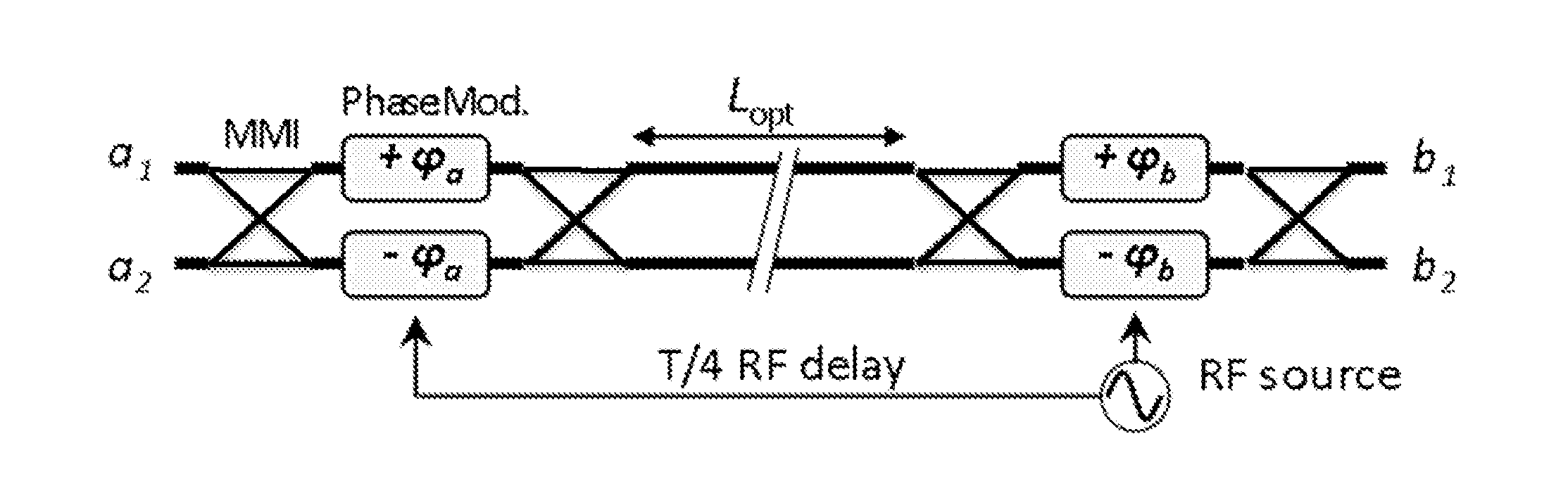
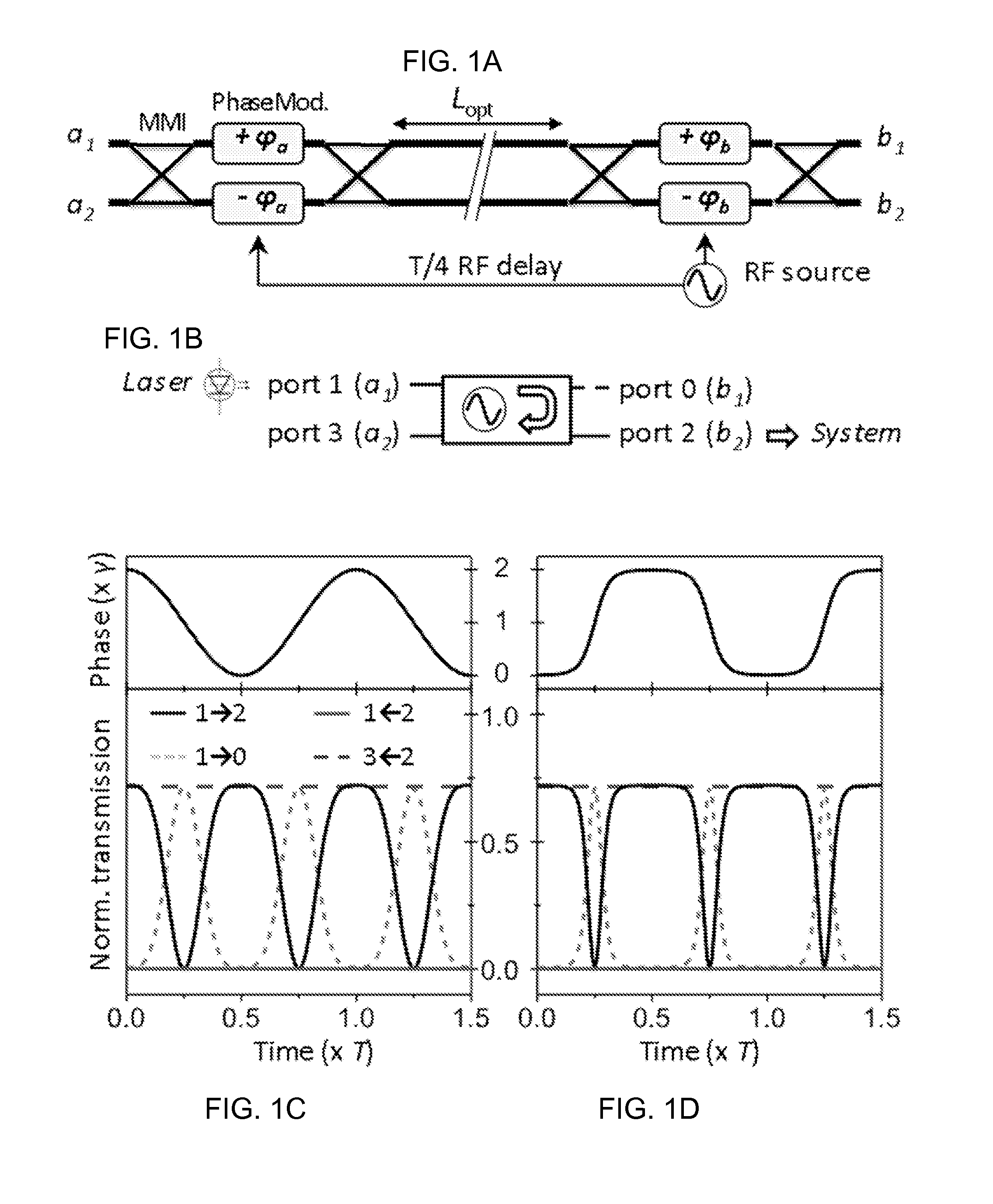
[0047]We describe a new non-reciprocal photonic circuit operating with standard singlemode waveguides or fibers. The non-reciprocal photonic circuit can be fabricated in processes compatible with the existing complementary metal-oxide-semiconductor (CMOS) infrastructure. The non-reciprocal photonic circuit exploits a time-dependent index modulation obtained with conventional phase modulators such as the one widely available in silicon photonics platforms. Because it is based on fully balanced interferometers and does not involve resonant structures, the non-reciprocal photonic circuit is also intrinsically broadband. Using realistic parameters we calculate an extinction ratio superior to 20 dB and insertion loss below −5 dB.

[0048]FIG. 1A is an illustration of a single module of the invention functioning as a nonreciprocal modulator, as it can be implemented in a PIC.

[0049]FIG. 1B is a schematic illustration of the input and output relations for the nonreciprocal modulator of FIG. 1A...


PUM

PropertyMeasurementUnit
insertion lossaaaaaaaaaa

Abstract

Optical devices that do not employ magneto-optics materials or non-linear effects to achieve non-reciprocal light propagation. The optical devices are compatible with the fabrication of monolithic photonic integrated circuits such as silicon-on-insulator planar lightwave circuits. In particular the devices use demonstrated passive (beam-splitters, waveguides) and active (phase modulators) components to achieve non-reciprocal light propagation. The devices can be used as non-reciprocal optical modulators or optical isolators when driven by a periodic radio frequency (RF) electric source.

Description

CROSS-REFERENCE TO RELATED APPLICATIONS[0001]This application claims priority to and the benefit of co-pending U.S. provisional patent application Ser. No. 61 / 820,274, filed May 7, 2013, which application is incorporated herein by reference in its entirety.FIELD OF THE INVENTION[0002]The invention relates to optical devices in general and particularly to an optical isolator.BACKGROUND OF THE INVENTION[0003]Optical isolators are nonreciprocal devices that allow the passage of light in one direction and block light in the other direction. They are useful components in optical systems, including telecommunication networks and many opto-electronic devices. For example, they are often placed at the output of laser sources to protect them from back reflection. Existing technologies employed in commercial optical isolators use a material with a large magneto-optic coefficient. The magneto-optic (Faraday) effect causes a propagation-direction-dependent rotation of the light polarization. Va...

Claims


Application Information

Patent Timeline
Patent Type & Authority Applications(United States)
IPC IPC(8): G02F1/225
CPCG02F1/225G02F2001/212G02B6/12007G02B6/2746G02F1/212
Inventor GALLAND, CHRISTOPHEBAEHR-JONES, THOMAS
Owner NOKIA SOLUTIONS & NETWORKS OY
Why Eureka
Try Eureka