Base metal combination electrode of electronic ceramic component and manufacturing method thereof
a technology of electronic ceramic components and base metals, applied in resistive material coatings, conductors, fixed capacitor details, etc., can solve the problems of high cost of silver electrode materials, sharp increase in voltage in circuits, and low varistor performance, and achieve simple technological process, high preparation efficiency, and reduced electrode material cost
- Summary
- Abstract
- Description
- Claims
- Application Information
AI Technical Summary
Benefits of technology
Problems solved by technology
Method used
Image
Examples
embodiment 1
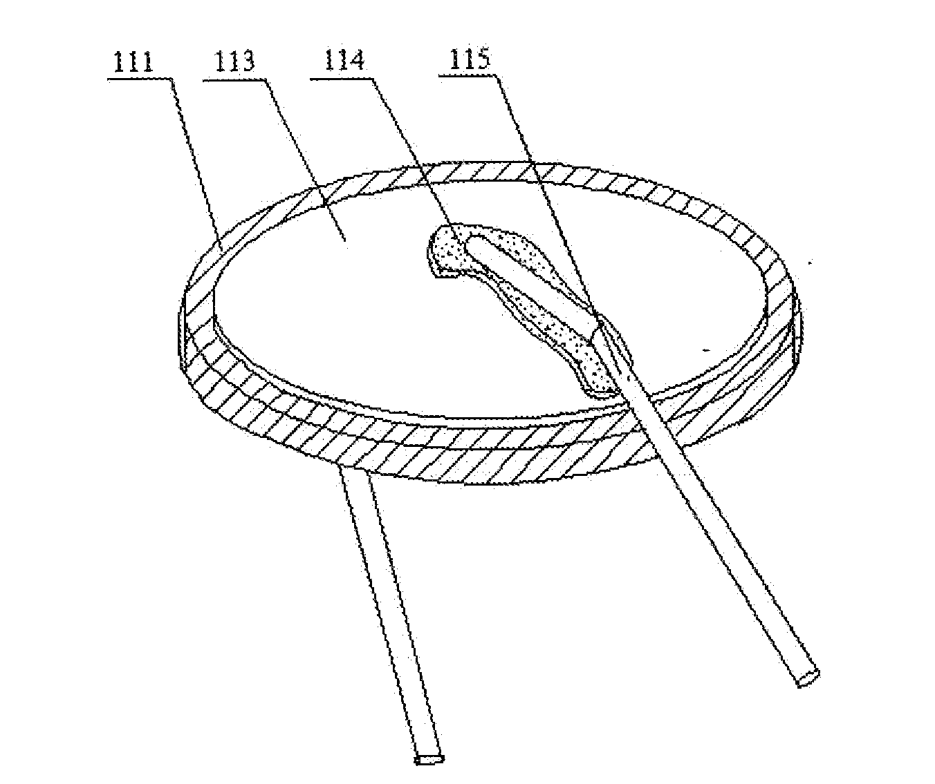
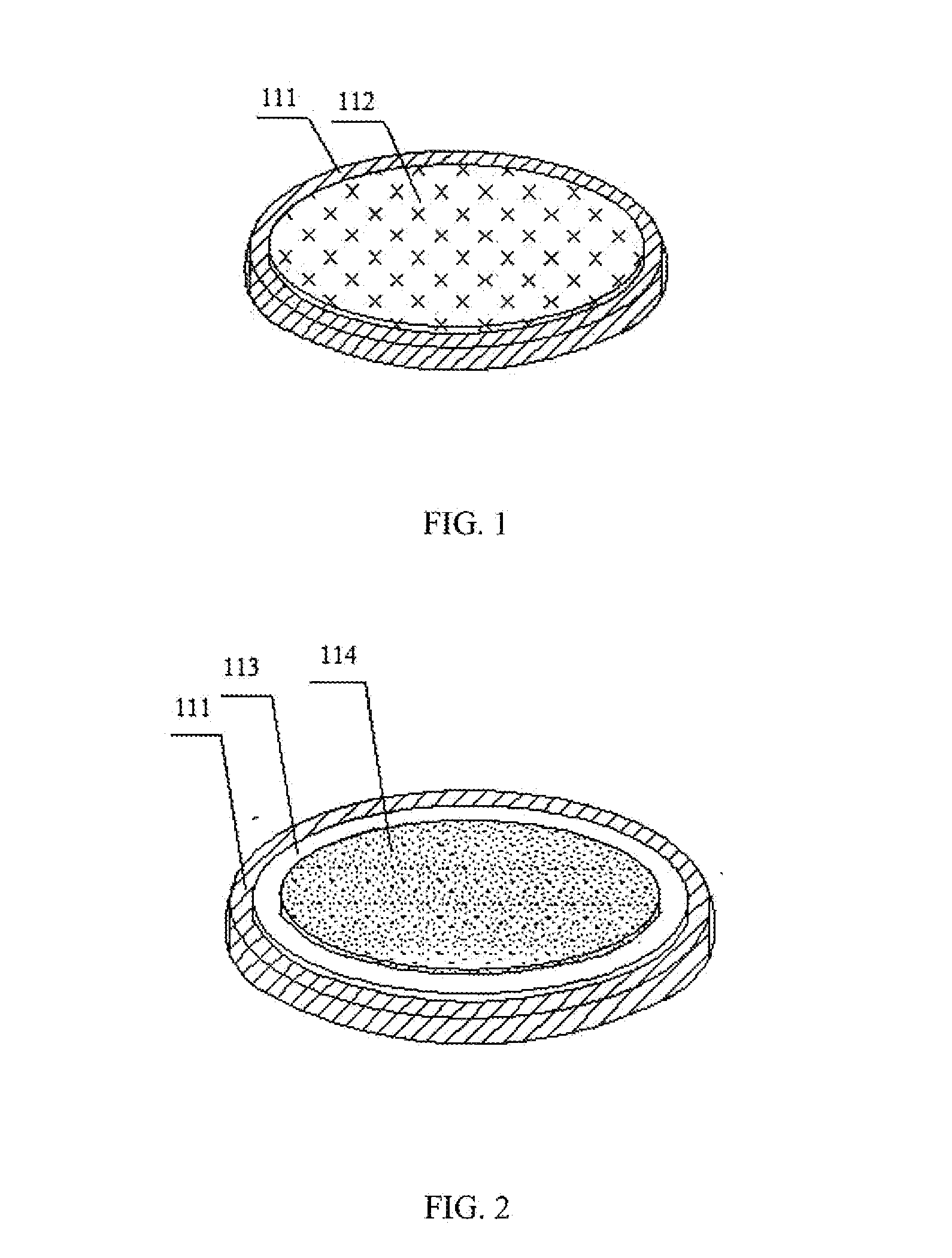
[0069]FIG. 2 is a structure diagram of the base metal combination electrode of electronic ceramic component of embodiment 1 of the present invention. As shown in FIG. 2, said electronic ceramic component comprises an electronic ceramic chip 111 and a base metal combination electrode 113,114, said electronic ceramic chip 111 refers to a ceramic body without the electrode layer coating, said base metal combination electrode comprises a first base metal electrode layer 113 covering on two sides of said electronic ceramic chip and a second base metal electrode layer 114 covering on said first base metal electrode layer. Said second base metal electrode layer 114 is a weld layer.
[0070]In this embodiment, said first base metal electrode layer 113 is made of aluminum electrode material, and said second base metal electrode layer 114 is made of copper electrode material, thus, said first base metal electrode layer 113 is an aluminum electrode layer 113, and said second base metal electrode ...
embodiment 2
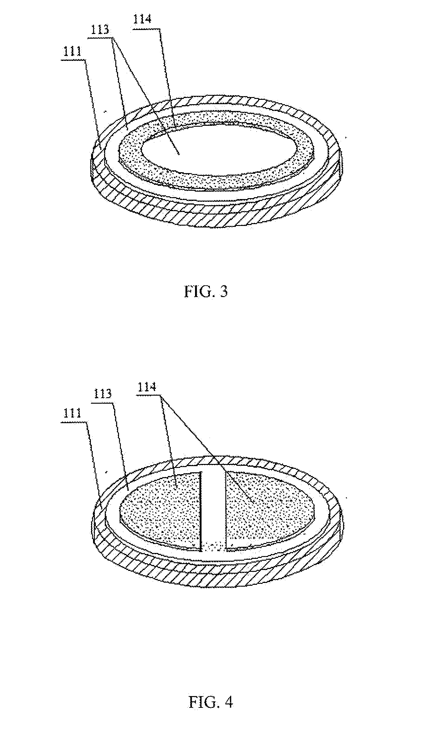
[0076]FIG. 3 is a structure diagram of base metal combination electrode of electronic ceramic component of embodiment 2 of the present invention. This embodiment is different from Embodiment 1 only in that:
[0077]In this embodiment, said first base metal electrode layer 113 is made of aluminum electrode material, and said second base metal electrode layer 114 is made of zinc electrode material, thus, said first base metal electrode layer 113 is an aluminum electrode layer 113, and said second base metal electrode layer 114 is a zinc electrode layer 114.
[0078]Besides, as shown in FIG. 3, said zinc electrode layer 114 is annular. In this embodiment, the annular has a width of 2 mm at least and 30 mm at most.
embodiment 3
[0079]FIG. 4 is a structure diagram of the base metal combination electrode of electronic ceramic component of embodiment 3 of the present invention. This embodiment is different from Embodiment 1 only in that:
[0080]In this embodiment, said first base metal electrode layer 113 is made of aluminum electrode material, and said second base metal electrode layer 114 is made of tin electrode material, thus, said first base metal electrode layer 113 is an aluminum electrode layer 113, and said second base metal electrode layer 114 is a tin electrode layer 114.
[0081]Besides, as shown in FIG. 4, said tin electrode layer 114 covering on one side of the electronic ceramic chip 111 comprises a plurality of covering portions separated from each other. In this embodiment, said tin electrode layer 114 comprises two half-round covering portions, the separation distance between which is more than 1 mm.
PUM
| Property | Measurement | Unit |
|---|---|---|
| Fraction | aaaaa | aaaaa |
| Time | aaaaa | aaaaa |
| Mechanical strength | aaaaa | aaaaa |
Abstract
Description
Claims
Application Information


