Eureka AIR delivers breakthrough ideas for toughest innovation challenges, trusted by R&D personnel around the world.

Double-sided transparent conductive film and touch panel

Active Publication Date: 2014-11-27
NITTO DENKO CORP
View PDF15 Cites 10 Cited by
  • Summary
  • Abstract
  • Description
  • Claims
  • Application Information

AI Technical Summary

Benefits of technology

The patent describes a double-sided transparent conductive film that has good anti-blocking properties and a smooth surface. The film has a base material film with protrusions that are formed by particles. The film also has an anti-blocking layer with flat portions and protrusion portions. The protrusions are caused by particles and are formed when the anti-blocking layer is wet coated. The film is made using various plastic films that have transparency. The thickness of the base material film is preferably in a range of 2 to 200 μm. The surface of the base material film may be treated to improve adhesion with the anti-blocking layer and the optical adjusting layer. The technical effects of the patent are that the double-sided transparent conductive film has good anti-blocking properties and a smooth surface, and the film is easy to manufacture.

Problems solved by technology

However, in the roll-to-roll manner, films superimposed onto each other may adhere closely to each other and may become hard to be peeled from each other (the so-called blocking).
In some cases, the films may be broken or scratched to be declined in productivity.
However, when an optical adjusting layer is formed onto the anti-blocking layer through a wet coating process, the protrusion portions of the anti-blocking layer are lost by a liquid for the coating so that this layer does not exhibit anti-blocking property.

Method used


Image

  • Double-sided transparent conductive film and touch panel
  • Double-sided transparent conductive film and touch panel

Examples


example 1

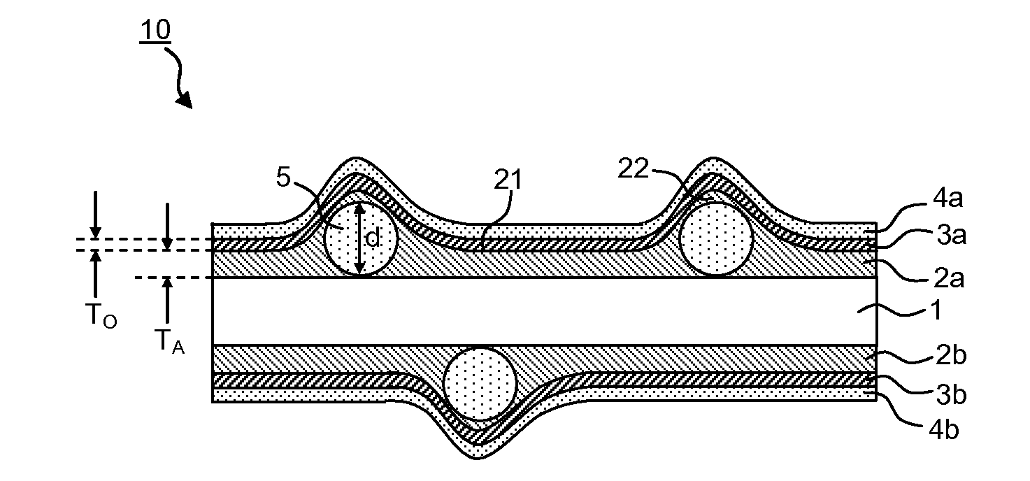
[0074]Prepared was a coating composition containing a plurality of mono-dispersible particles (manufactured by Soken Chemical Engineering Co., Ltd., trade name “SX-130H”) having a mode diameter of 1.3 μm, a binder resin (manufactured by DIC Corporation, trade name “UNIDIC RS29-120”), and ethyl acetate as a solvent. The addition amount of the particles was 0.2 parts based on 100 parts of the binder resin. Next, a gravure coater was used to apply the coating composition onto the both sides of a long base material film (manufactured by Nippon Zeon Co., Ltd., trade name “ZEONOA”) having a thickness of 100 μm in such a manner that the applied films would each have a thickness of 1.0 μm after dried. The workpiece was heated at 80° C. for 1 minute to dry the applied films. Thereafter, the workpiece was irradiated with ultraviolet rays giving a cumulative light quantity of 250 mJ / cm2 from a high-pressure mercury lamp to form anti-blocking layers.

[0075]Next, a gravure coater was used to appl...

example 2

[0078]A double-sided transparent conductive film was prepared in the same manner as in Example 1 except that monodisperse particles having a mode diameter of 1.5 μm (manufactured by SEKISUI PLASTICS CO., Ltd., trade name “XX-184AA”) were used as particles, and the added amount of the particles was 0.3 parts based on 100 parts of the binder resin.

example 3

[0079]A double-sided transparent conductive film was prepared in the same manner as in Example 1 except that monodisperse particles having a mode diameter of 1.9 μm (manufactured by Soken Chemical Engineering Co., Ltd., trade name “MX-180TA”) were used as particles, and the added amount of the particles was 0.2 parts based on 100 parts of the binder resin.


PUM

PropertyMeasurementUnit
Transparencyaaaaaaaaaa
Nanoscale particle sizeaaaaaaaaaa

Abstract

Provided are a double-sided transparent conductive film which is good in appearance even when its transparent conductive layers are patterned, and has anti-blocking property, thereby being producible at low costs; a wound body thereof; and a touch panel. The double-sided transparent conductive film includes a base material film, and a base material film, and an optical adjusting layer and a transparent conductive layer which are formed in this order on each of both sides of the base material film, wherein an anti-blocking layer containing particles is formed at least one of: a location between the base material film and one optical adjusting layer; and a location between the base material film and the other optical adjusting layer, the anti-blocking layer has a flat portion and protrusion portions caused by the particles, and a value obtained by subtracting a thickness of the flat portion of the anti-blocking layer from a mode diameter of the particles is larger than a thickness of the optical adjusting layer.

Description

BACKGROUND OF THE INVENTION[0001]1. Field of the Invention[0002]The present invention relates to a double-sided transparent conductive film, and a touch panel.[0003]2. Description of the Related Art[0004]In recent years, projected-capacitive touch panels or matrix-type resistive touch panels can attain multi-point input (multi-touch) to be excellent in operability. Demands therefor have been rapidly increasing. As an electrode member of such a touch panel, a double-sided transparent conductive film is suggested, in which transparent conductive thin films are formed on both sides of a transparent film base material, respectively.[0005]A touch panel as described above makes use of a double-sided transparent conductive film having patterned transparent conductive layers. As the material of the transparent conductive layers, indium / tin composite oxide (ITO) is widely used from the viewpoint of the visible ray transmittance thereof. However, the refractive index of ITO is high. Thus, whe...

Claims


Application Information

Patent Timeline
IPC IPC(8): H01B5/00H01B1/08H05K1/02H01B5/14
CPCH01B5/002H01B5/14H05K1/0298H05K1/0274H01B1/08G06F3/0412G06F2203/04103Y10T428/24364G06F3/044G06F3/045G06F3/041
Inventor TAKADA, KATSUNORIHASHIMOTO, NAOKIHIRAOKA, SHINYAIKAI, KAZUHIROKURAMOTO, HIROKITAKAO, HIROYUKITSUNO, NAOKIUMEMOTO, TORU
Owner NITTO DENKO CORP
Why Eureka
Eureka Blog
Learn More