

Organic semiconductor compositions
a semiconductor and organic technology, applied in the field of organic copolymer and organic semiconducting compositions, can solve the problems of limited practice, damage to the environment, and the method of preparing the ofets described
- Summary
- Abstract
- Description
- Claims
- Application Information
AI Technical Summary
Benefits of technology
Problems solved by technology
Method used
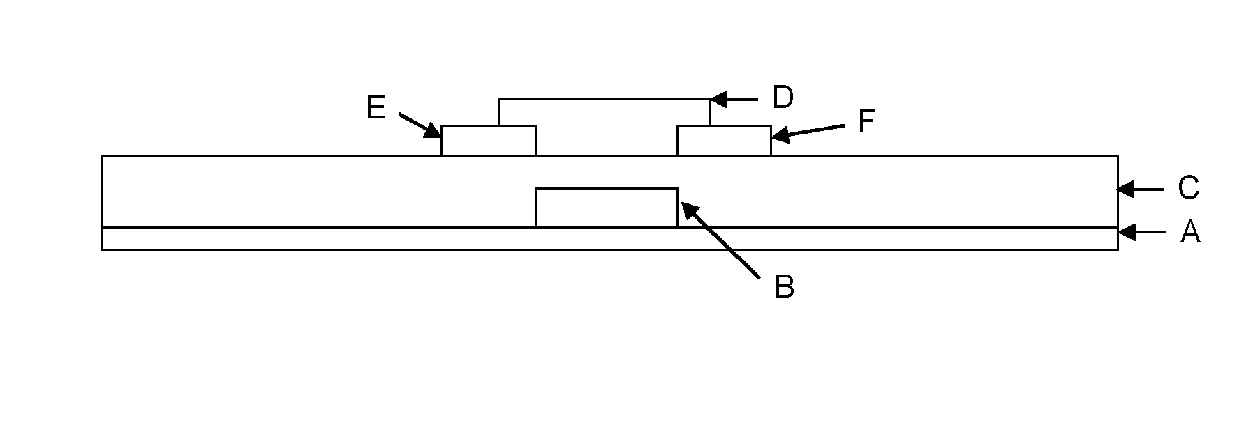
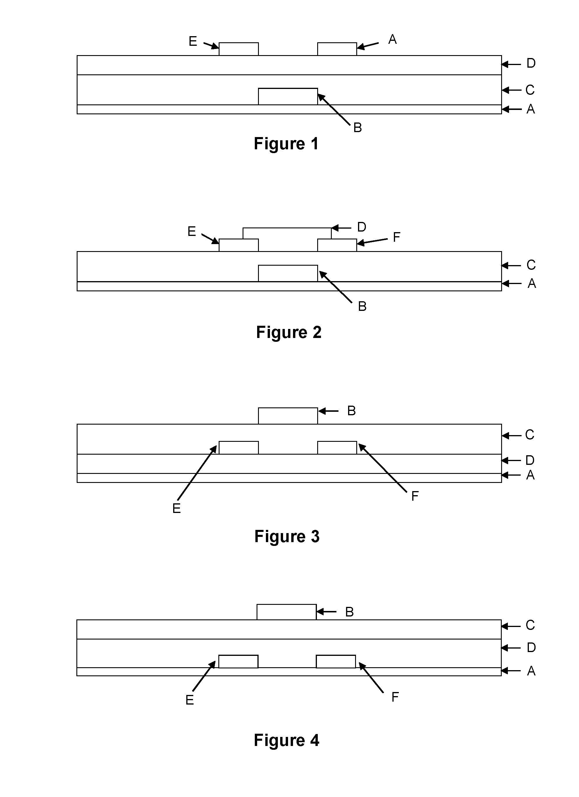
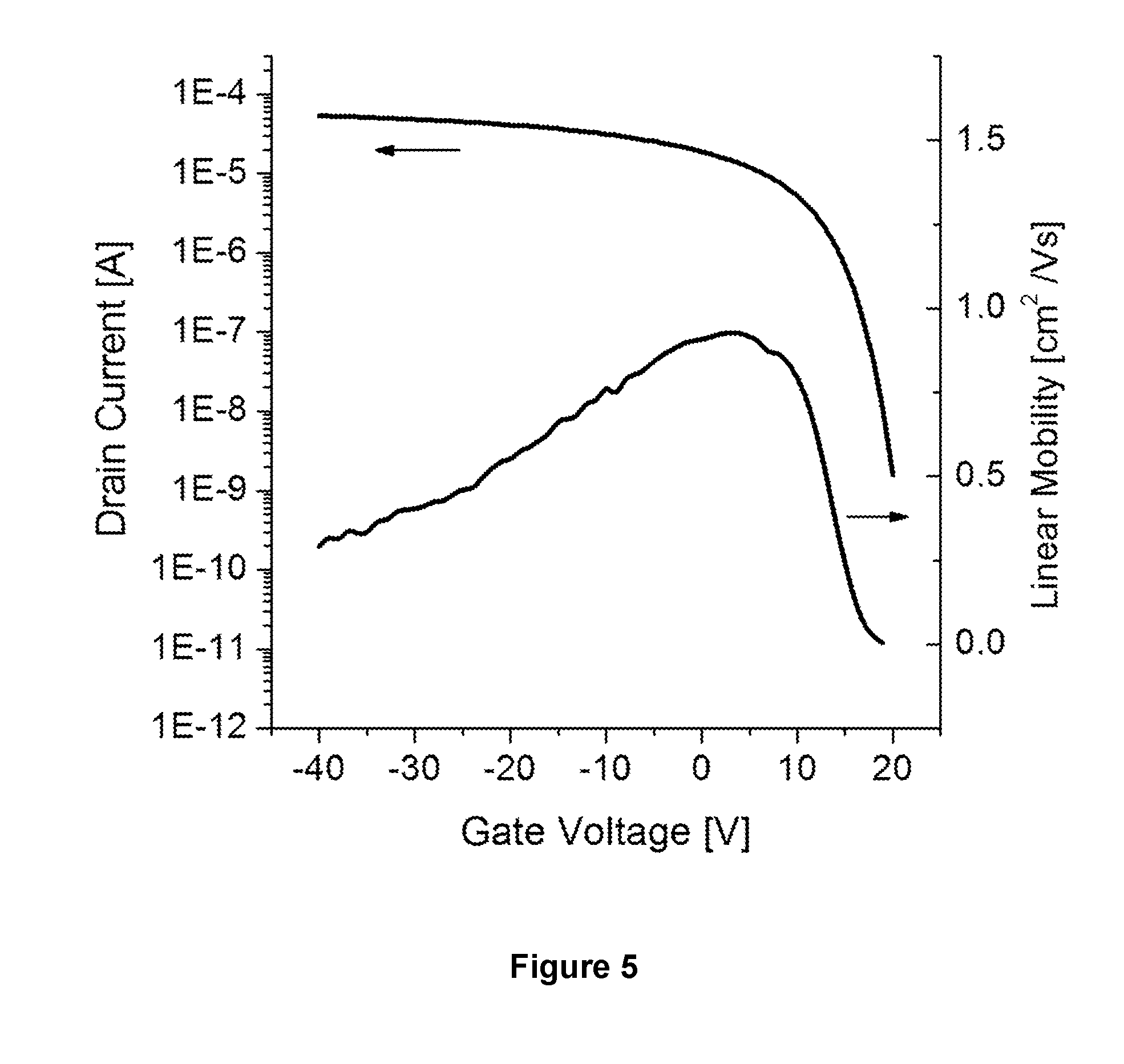
Image

Examples
example
(1)
PAHC (1): Preparation of TES-anthracenedithiophene-6,12-dihydro-6,6,12,12-tetraoctyl-indeno[1,2-b]fluorene copolymer
[0182]A mixture of 2,8-dibromo-5,11-bis(triethylsilylethynyl)anthra[2,3-b:6,7-b′]dithiophene / 2,8-dibromo-5,11-bis(triethylsilylethynyl)anthra[2,3-b:7,6-b′]dithiophene(4) (0.20 g, 0.28 mmol, 0.5 eq), 2,8-Dibromo-6,12-dihydro-6,6,12,12-tetraoctyl-indeno[1,2-b]fluorene (Sigma-Aldrich 708267, 0.24 g, 0.28 mmol, 0.5 eq), 2,8-bis[(4,4,55-tetramethyl-1,3,2-dioxaborolan-2-yl)]-6,12-dihydro-6,6,12,12-tetraoctyl-indeno[1,2-b]fluorene(5) (0.53 g, 0.55 mmol, 1 eq), tetrakis(triphenylphosphine)palladium (0) (Acros 12065360, 0.022 g, 0.02 mmol, 0.03 eq), 2M K2CO3 (1.7 mL, 3.4 mmol, 6 eq) and Aliquat® 336 (Sigma-Aldrich 205613, 8 drops) in toluene (40 mL) was degassed by passing a stream of nitrogen through the solution for 30 minutes. The mixture was then heated to reflux. After 2 hours HPLC confirmed the presence of oligomers. The reaction mixture was allowed to cool to 50 deg C...
PUM
| Property | Measurement | Unit |
|---|---|---|
| channel lengths | aaaaa | aaaaa |
| dielectric constant | aaaaa | aaaaa |
| channel lengths | aaaaa | aaaaa |
Abstract
Description
Claims
Application Information