Method for growing germanium/silicon-germanium superlattice

a technology of germanium and germanium, which is applied in the direction of crystal growth process, polycrystalline material growth, radiofrequency control device, etc., can solve the problems of high cost, incompatibility with silicon processing, and difficulty in growing single-crystal germanium on silicon substrates, etc., to reduce temperature and pressure, the effect of reducing the temperatur

Active Publication Date: 2015-01-29
BAE SYST INFORMATION & ELECTRONICS SYST INTERGRATION INC
View PDF1 Cites 6 Cited by
  • Summary
  • Abstract
  • Description
  • Claims
  • Application Information

AI Technical Summary

Benefits of technology

[0004]An embodiment provides a method of growing a germanium/silicon-germanium strained-layer superlattice structure comprising the steps of (a) preconditioning a silicon substrate with hydrogen gas with a pressure at most equal to approximately 3E−4 mBar; (b) reducing temperature and pressure; (c) providing germane gas with a pressure at most equal to approximately 5E−4 mBar flowing over the silicon substrate to form a germanium seed layer; (d) heating in approximately a vacuum; (e) flowing gasses with a pressure at most equal to approximately 5E−4 mBar over the germanium seed layer to form a doped germanium layer; (f) flowing germane gas with a pressure at most equal to approximately 5E−4 mBar over the germanium layer forming a first buffer; (g) flowing at least germane gas over the first buffer with a pressure at most equal to approximately 5E−4 mBar, forming a layer of single-crystal comprising at least germanium; (h) flushing with hydrogen or allowing to remain idle; (i) flowing gasses over the single-crystal comprising at least germanium layer with a pressure at most approximately 5E−4 mBar, forming a subsequent layer of single-crystal silicon-germanium; (j) flushing with hydrogen or allowing to remain idle; (k) repeating steps (g) through (j) multiple times, forming SLS layers (at least one of the alternating layers is silicon-germanium); (1) flowing germane gas with a pressure at most equal to approximately 5E−4 mBar over a germanium layer forming a second buffer; and (m) flowing gasses with a pressure at most equal to approximately 5E−4 mBar over the second buffer to form a doped layer. In embodiments, in step (a) preconditioning occurs at approximately 750° C. for approximately 60 minutes. In other embodiments, in step (b) the temperature is reduced to approximately 350° C. and the pressure is reduced to approximately vacuum. In subsequent embodiments the temperature is reduced at a rate of approximately 2° C./min. For additional embodiments, in step (c) the germane gas is flowed over the silicon substrate for approximately 120 minutes. In another embodiment, in step (d) the heating occurs at approximately 2° C./min until the temperature is approximately 600° C. In included embodiments, in step (e) the gasses are selected from the group consisting of phosphine, diborane and germane for an n-doped layer, or selected from the group consisting of germane and diborane for a p-doped layer. In yet further embodiments, in step (e) the phosphine and germane gasses are provided at a ratio of approximately 1:3 respectively for approximately 10 minutes. Embodiments further provide that in step (e) the phosphine and germane gasses are provided such that the germanium seed layer is doped with phosphorus at a concentration of approximately 1E18 atoms/cm3. For a following embodiment, step (f) occurs for approximately 20 minutes, step (g) occurs for approximately 1 minute, and step (h) occurs for approximately 2 minutes. In subsequent embodiments, in steps g and i, at least one gas is selected from the group consisting of silane and germane (at least one of the alternating layers is silicon-germanium). In additional embodiments, in step (i) the gasses are provided in a 4:1 ratio of silane and germane. In included embodiments step (i) occurs for approximately 90 seconds, step (1) occurs for approximately 20 minutes, and step (m) occurs for approximately 30 minutes. Another embodiment provides that in step (m) the gasses are selected from the group consisting of germane and diborane for a p-doped layer, or selected from the group consisting of phosphine, diborane and germane for an n-doped layer. In related embodiments, the gasses in step (m) occur at approximately a 1:50 ratio. For further embodiments, in step (m) a p-doped layer comprises a boron concentration of 5E17 atoms/cm3. In yet further embodiments, steps (g)-(j) are repeated to form at least 2 layers.
[0005]Another embodiment provides a method of growing a germanium/silicon-germanium superlattice structure (SLS) comprising (a) preconditioning a sil

Problems solved by technology

An existing material used for manufacturing short wave-infrared focal-plane arrays (SWIR FPA) is InGaAs, which is expensive and incompatible with silicon processing.
However, growing uniform single-crystal germanium on silicon substrate is a challenge due to silicon and germanium la

Method used


Image

  • Method for growing germanium/silicon-germanium superlattice
  • Method for growing germanium/silicon-germanium superlattice
  • Method for growing germanium/silicon-germanium superlattice

Examples


Embodiment Construction

[0010]The following detailed description provides example embodiments of the presently claimed invention with references to the accompanying drawings. The features and advantages described herein are not all-inclusive and, in particular, many additional features and advantages will be apparent to one of ordinary skill in the art in view of the drawings, specification, and claims. Moreover, it should be noted that the language used in the specification has been selected principally for readability and instructional purposes, and not to limit in any way the scope of the inventive subject matter. Embodiments are described in sufficient detail to enable one of ordinary skill in the art to practice the subject invention. The invention is susceptible of many embodiments. What follows is illustrative, but not exhaustive, of the scope of the invention.

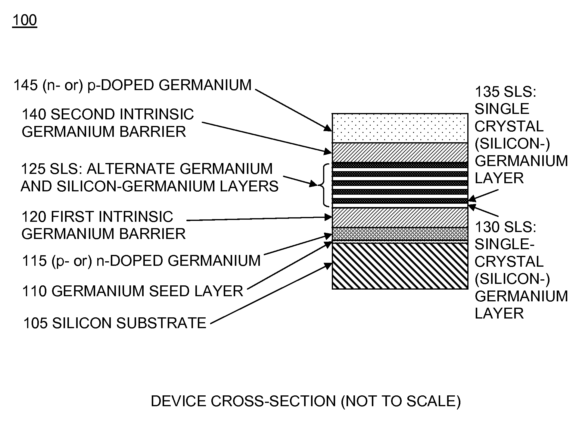
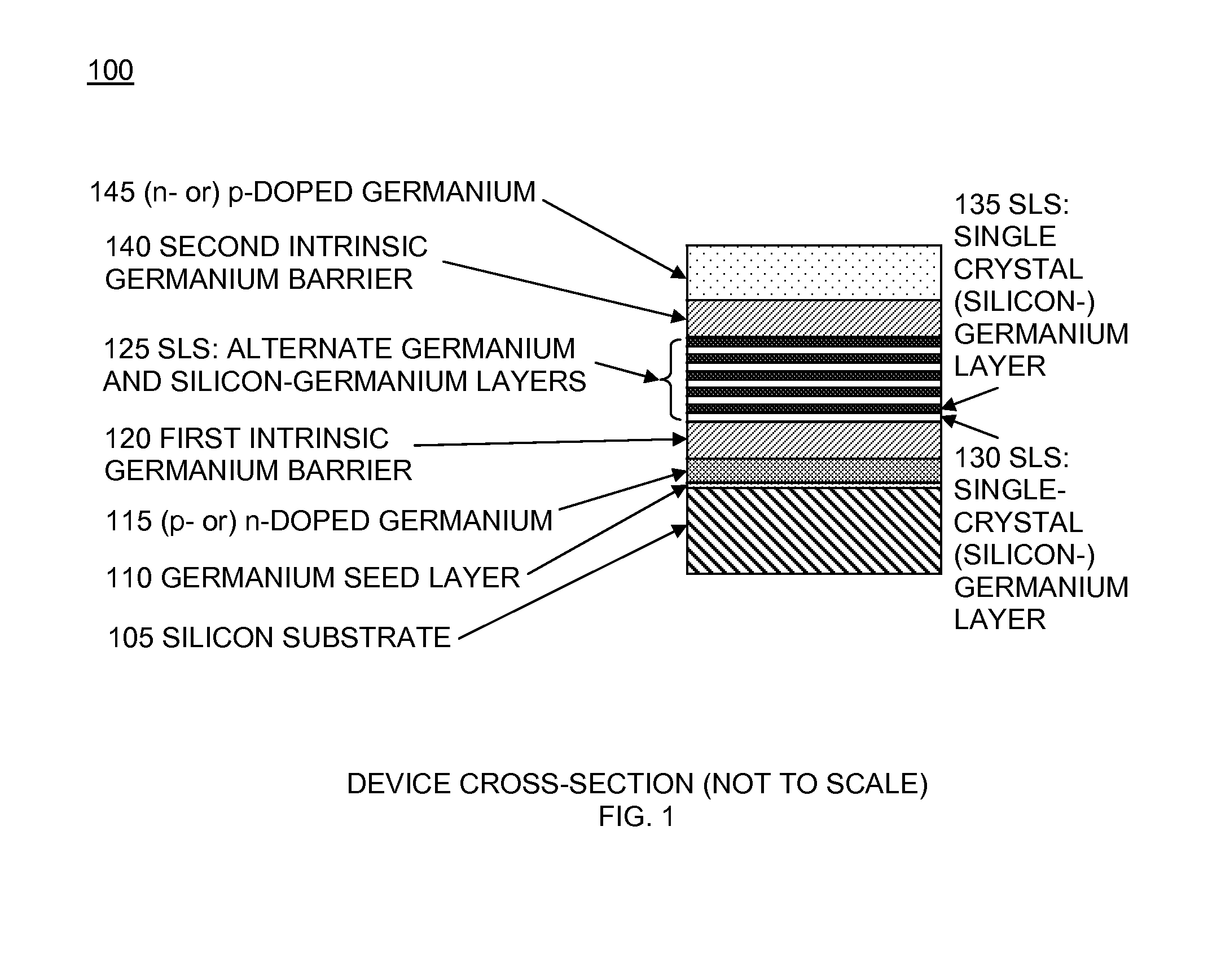
[0011]Embodiments provide a method of growing a p-SLS-n stack for making vertical p-i-n photodetectors using an ultra-high vacuum-chemical va...


PUM


Abstract

A bulk manufacturing method for growing silicon-germanium stained-layer superlattice (SLS) using an ultra-high vacuum-chemical vapor deposition (UHV-CVD) system and a detector using it is disclosed. The growth method overcomes the stress caused by silicon and germanium lattice mismatch, and leads to uniform, defect-free layer-by-layer growth. Flushing hydrogen between the layer growths creates abrupt junctions between superlattice structure (SLS) layers. Steps include flowing a mixture of phosphine and germane gases over a germanium seed layer. This in-situ doped germanium growth step produces an n-doped germanium layer. Some of the phosphorus diffuses into the underlying germanium and reduces the stress in the underlying germanium that is initially created by the lattice mismatch between germanium and silicon. Phosphine can be replaced by diborane if a p-doped layer is desired. The reduction of stress results in a smooth bulk germanium growth.

Description

RELATED APPLICATIONS[0001]This application claims the benefit of U.S. Provisional Application No. 61 / 858,649 filed Jul. 26, 2013. This application is herein incorporated by reference in its entirety for all purposes.FIELD OF THE INVENTION[0002]The invention relates to a device and a method for growing silicon-germanium superlattice structure on silicon substrates.BACKGROUND[0003]An existing material used for manufacturing short wave-infrared focal-plane arrays (SWIR FPA) is InGaAs, which is expensive and incompatible with silicon processing. Silicon-germanium strained-layer superlattice structure (Si:Ge SLS) is used as an alternative. However, growing uniform single-crystal germanium on silicon substrate is a challenge due to silicon and germanium lattice mismatch. Growing an ultrathin layer of germanium on top of a layer of silicon-germanium, or alternating layers of silicon-germanium with varying silicon content, with abrupt transitions for making hundreds of pairs of layers of st...

Claims


Application Information

Patent Timeline
IPC IPC(8): C30B25/16H01L31/111C30B29/06C30B29/68C30B29/52H01L31/028H01L27/146
CPCC30B25/165H01L31/028H01L31/111C30B29/06C30B29/68C30B29/52H01L27/14601H01L27/1446H01L31/035254H01L31/105H01L21/02507H01L21/02532
Inventor VU, VU ANHHYLAND, SANDRA L.KAMOCSAI, ROBERT L.O'DONNELL, DANIEL J.POMERENE, ANDREW T.
Owner BAE SYST INFORMATION & ELECTRONICS SYST INTERGRATION INC
Why Eureka
Try Eureka