Semiconductor device and method for manufacturing semiconductor device

a semiconductor device and semiconductor technology, applied in the direction of semiconductor devices, electrical devices, transistors, etc., can solve the problems of deterioration of the electrical characteristics of the transistor, and achieve the effects of suppressing the reduction of on-state current, deteriorating electrical characteristics, and high integration

Inactive Publication Date: 2015-02-05
SEMICON ENERGY LAB CO LTD
View PDF4 Cites 27 Cited by
  • Summary
  • Abstract
  • Description
  • Claims
  • Application Information

AI Technical Summary

Benefits of technology

[0023]One embodiment of the present invention can provide any of the following semiconductor devices: a semiconductor device in which deterioration of electrical characteristics, which becomes more noticeable with miniaturization, can be prevented; a highly integrated se

Problems solved by technology

Miniaturization of transistors may cause deterioration of the electrical characteristics of the transist

Method used


Image

  • Semiconductor device and method for manufacturing semiconductor device
  • Semiconductor device and method for manufacturing semiconductor device
  • Semiconductor device and method for manufacturing semiconductor device

Examples


embodiment 1

[0057]In this embodiment, a semiconductor device of one embodiment of the present invention will be described with reference to drawings.

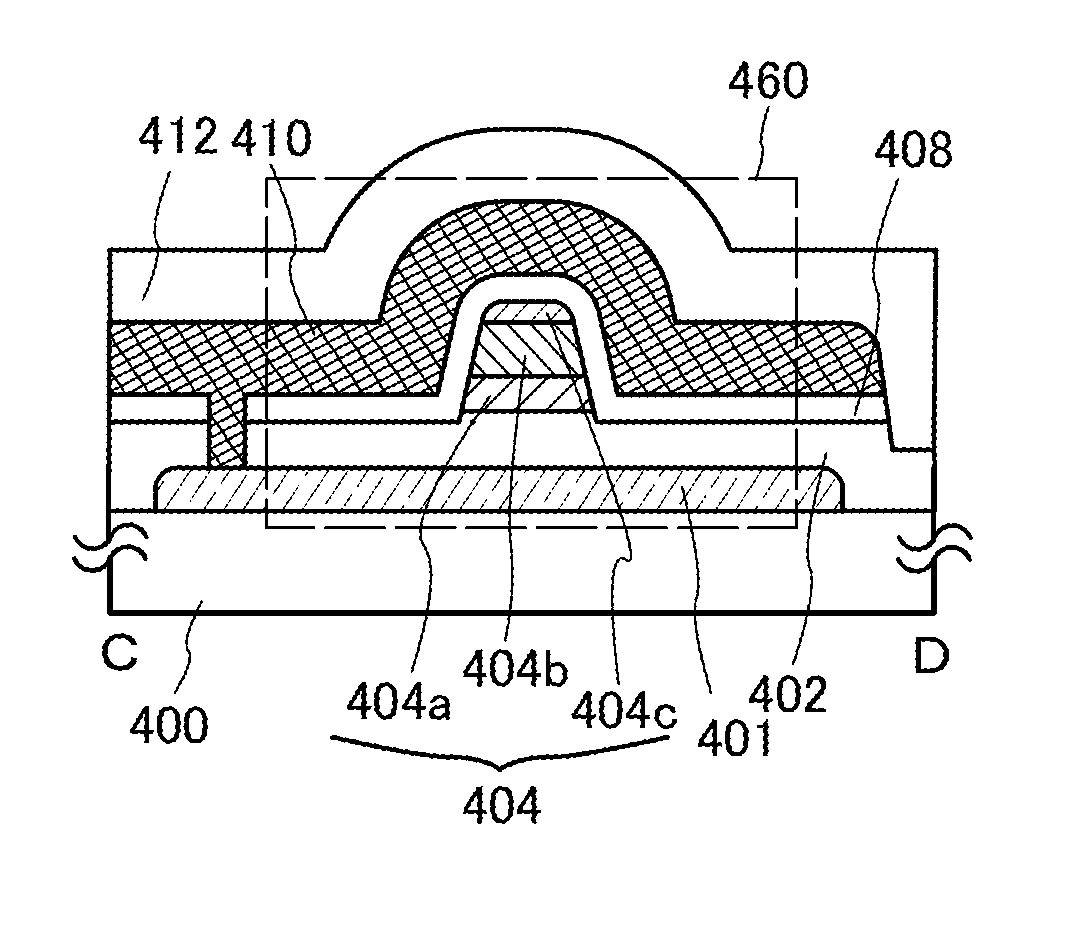
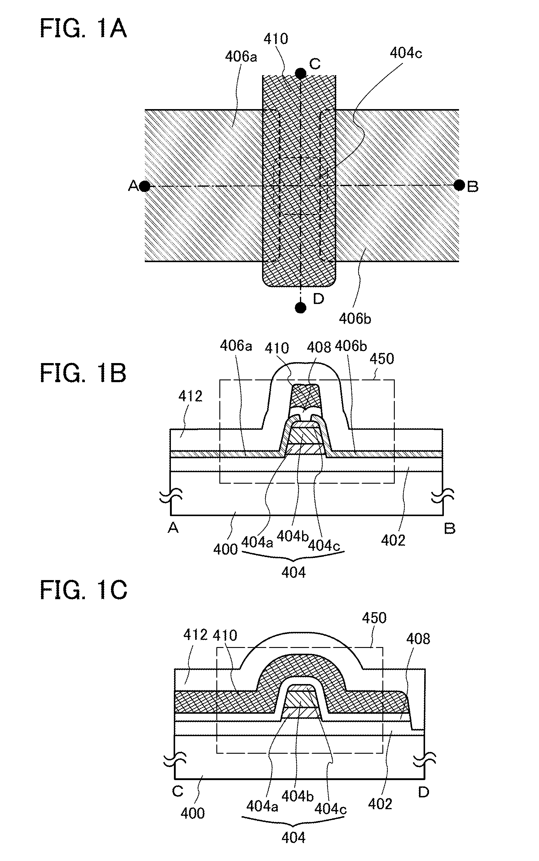
[0058]FIGS. 1A to 1C are a top view and cross-sectional views illustrating a transistor of one embodiment of the present invention. FIG. 1A is a top view. FIG. 1B illustrates a cross section taken along dashed-dotted line A-B of FIG. 1A. FIG. 1C illustrates a cross section taken along dashed-dotted line C-D of FIG. 1A. Note that some components are not illustrated in the top view of FIG. 1A for simplification. The direction of the dashed-dotted line A-B and the direction of the dashed-dotted line C-D can be referred to as a channel length direction and a channel width direction, respectively.

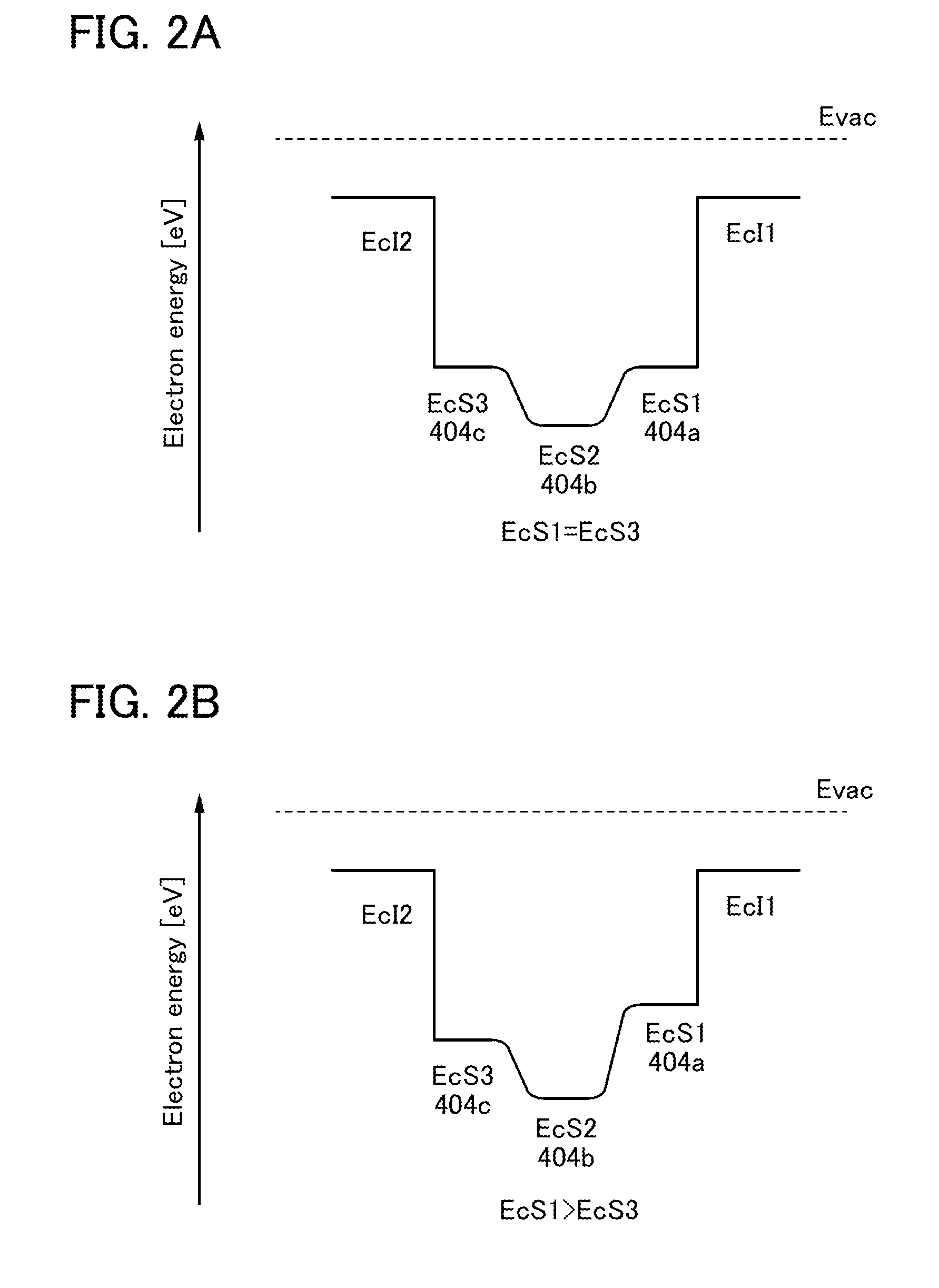
[0059]A transistor 450 illustrated in FIGS. 1A to 1C includes a base insulating film 402 having a depressed portion and a projected portion over a substrate 400; a first oxide semiconductor film 404a, a second oxide semiconductor film 404b, and a third oxide se...

embodiment 2

[0154]In this embodiment, a method for manufacturing the transistor 450 described in Embodiment 1 with reference to FIGS. 1A to 1C will be described with reference to FIGS. 7A to 7C and FIGS. 8A to 8C.

[0155]First, the base insulating film 402 is formed over the substrate 400 (see FIG. 7A).

[0156]As the substrate 400, a glass substrate, a ceramic substrate, a quartz substrate, a sapphire substrate, or the like can be used. Alternatively, a single crystal semiconductor substrate or a polycrystalline semiconductor substrate made of silicon, silicon carbide, or the like, a compound semiconductor substrate made of silicon germanium or the like, a silicon-on-insulator (SOI) substrate, or the like can be used. Further alternatively, any of these substrates further provided with a semiconductor element may be used.

[0157]The base insulating film 402 can be formed by a plasma CVD method, a sputtering method, or the like using an oxide insulating film of aluminum oxide, magnesium oxide, silicon...

embodiment 3

[0220]In this embodiment, a transistor having a structure different from that of the transistor described in the above embodiments will be described.

[0221]FIGS. 11A to 11C are a top view and cross-sectional views illustrating a transistor of one embodiment of the present invention. FIG. 11A is the top view. FIG. 11B illustrates a cross section taken along dashed-dotted line A-B in FIG. 11A. FIG. 11C illustrates a cross section taken along dashed-dotted line C-D in FIG. 11A. Note that for simplification of the drawing, some components in the top view in FIG. 11A are not illustrated. In some cases, the direction of the dashed-dotted line A-B is referred to as a channel length direction, and the direction of the dashed-dotted line C-D is referred to as a channel width direction.

[0222]A transistor 550 illustrated in FIGS. 11A to 11C includes the base insulating film 402 having the depressed portion and the projected portion over the substrate 400; the first oxide semiconductor film 404a...


PUM


Abstract

Provided is a semiconductor device having a structure which can prevent deterioration of the electrical characteristics, which becomes more significant with miniaturization. The semiconductor device includes a first oxide semiconductor film over an insulating surface; a second oxide semiconductor film over the first oxide semiconductor film; a third oxide semiconductor film over the second oxide semiconductor film; a source electrode and a drain electrode each in contact with side surfaces of the first oxide semiconductor film, the second oxide semiconductor film, and the third oxide semiconductor film and a top surface of the third oxide semiconductor film; a gate insulating film over the third oxide semiconductor film, the source electrode, and the drain electrode; and a gate electrode which is on and in contact with the gate insulating film and faces a top surface and a side surface of the second oxide semiconductor film.

Description

BACKGROUND OF THE INVENTION[0001]1. Field of the Invention[0002]The present invention relates to an object, a method, or a manufacturing method. The present invention relates to a process, a machine, manufacture, or a composition of matter. In particular, one embodiment of the present invention relates to a semiconductor device or a method for manufacturing a semiconductor device.[0003]In this specification, a semiconductor device generally means a device which can function by utilizing semiconductor characteristics. A display device, an electro-optical device, a semiconductor circuit, and an electric device may include a semiconductor device.[0004]2. Description of the Related Art[0005]Attention has been focused on a technique for formation of a transistor using a semiconductor thin film formed over a substrate having an insulating surface. The transistor is used in a wide range of electronic devices such as an integrated circuit (IC) and an image display device (display device). A...

Claims


Application Information

Patent Timeline
IPC IPC(8): H01L29/10H01L29/66H01L29/06H01L29/786
CPCH01L29/1054H01L29/7869H01L29/0657H01L29/66969H01L29/78696H01L27/1225
Inventor YAMAZAKI, SHUNPEI
Owner SEMICON ENERGY LAB CO LTD
Why Eureka
Try Eureka