
AlN SINGLE CRYSTAL SCHOTTKY BARRIER DIODE AND METHOD OF PRODUCING THE SAME

Inactive Publication Date: 2015-02-05
NAT INST FOR MATERIALS SCI
View PDF1 Cites 0 Cited by
  • Summary
  • Abstract
  • Description
  • Claims
  • Application Information

AI Technical Summary

Benefits of technology

The present invention provides an AlN single crystal Schottky barrier diode with excellent rectifying properties at high temperatures. The diode has a low on-resistance characteristic, allowing a current to flow at low voltages. The method of producing the diode involves producing a high-quality AlN single crystal, polishing it to a high-quality substrate, and then forming electrodes on one surface of the substrate using deposition or sputtering methods. The resulting diode has a high voltage resistance and can withstand high temperatures.

Problems solved by technology

However, the AlN used in the diode is one formed as a thin film on a SiC substrate through heteroepitaxial growth, and is not a bulk single crystal of good quality.
Further, the AlN diode is a p-n junction diode, and is not suitable for power diodes, since the ON resistance theoretically increases as compared with the Schottky barrier diode which is a power diode.
Production of high quality AlN single crystals is difficult and the device integration thereof is difficult, and thus the AlN Schottky diode operation has not been conventionally confirmed.
However, the AlN single crystal has not been reported as having semiconductor properties which may be used to form a Schottky barrier diode.

Method used


Image

  • AlN SINGLE CRYSTAL SCHOTTKY BARRIER DIODE AND METHOD OF PRODUCING THE SAME
  • AlN SINGLE CRYSTAL SCHOTTKY BARRIER DIODE AND METHOD OF PRODUCING THE SAME
  • AlN SINGLE CRYSTAL SCHOTTKY BARRIER DIODE AND METHOD OF PRODUCING THE SAME

Examples


example 1

Production of AlN Single Crystal Schottky Barrier Diode

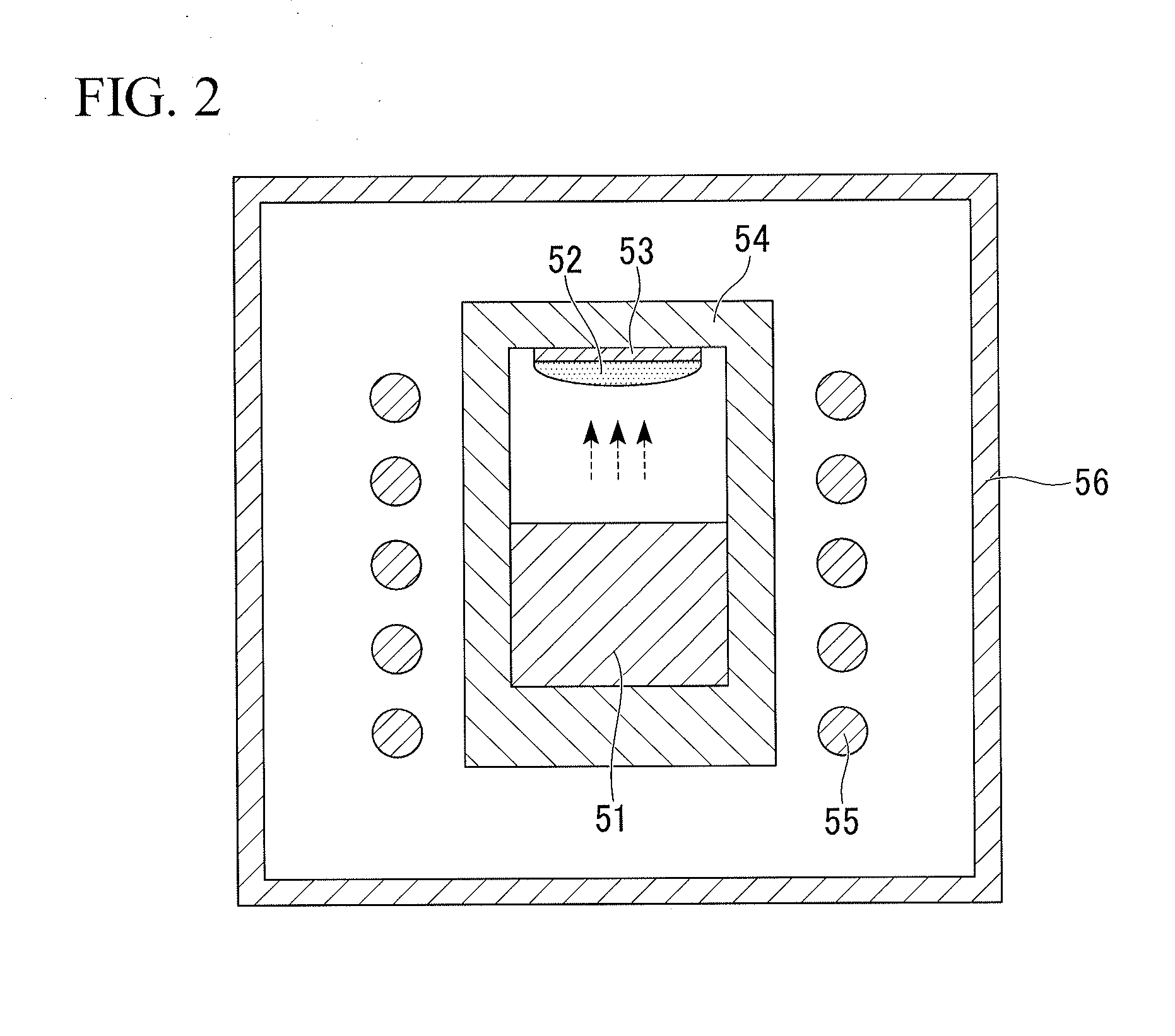
[0102]First, an AlN single crystal was produced by a sublimation method.

[0103]The production conditions in the sublimation method and the configuration of the produced AlN single crystal are shown in Table 1.

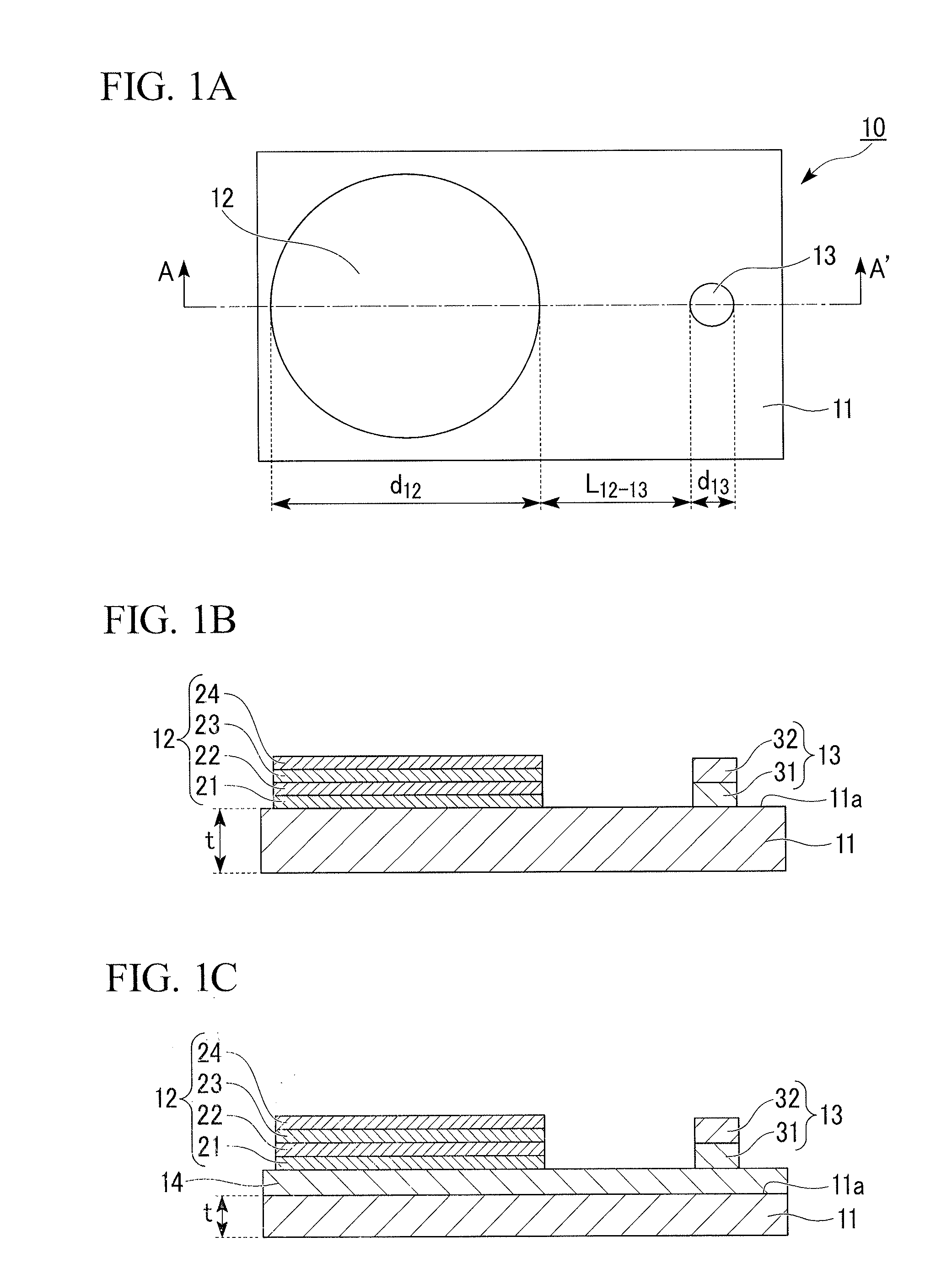
[0104]A cylindrical vessel having a diameter (inner diameter) of 10 mm and a depth of 50 mm was used as a crystal growth vessel. A SiC substrate having a diameter of 5 mm and an AlN raw material powder of high purity were enclosed inside the vessel and heated for 10 hours at a heating temperature of 2,000° C. in an RF furnace. As a result, an AlN single crystal having a diameter of 5 mm and a thickness of 0.5 mm was formed on the substrate.

TABLE 1Crystal growth vesselShapeCylindricalDiameter (mm)10Depth (mm)50Raw material heating temperature (° C.) 2,000Raw material heating time (hours)10Crystal growth substrate Diameter (mm)5AIN single crystalDiameter (mm)5Thickness (mm)0.5

[0105]Then, the obtained AlN single crystal was rem...

example 2

[0118]An Al single crystal (first AlN single crystal layer) was formed on a substrate under the same conditions as those in Example 1 with the exception that the heating time at the time of crystal growth was set to 24 hours. After cooling the substrate to room temperature, on the aforementioned Al single crystal, an Al single crystal (second AlN single crystal layer) was grown by setting the heating time to 24 hours once again. As a result, an MN single crystal thicker than that of Example 1 was obtained.


PUM


Abstract

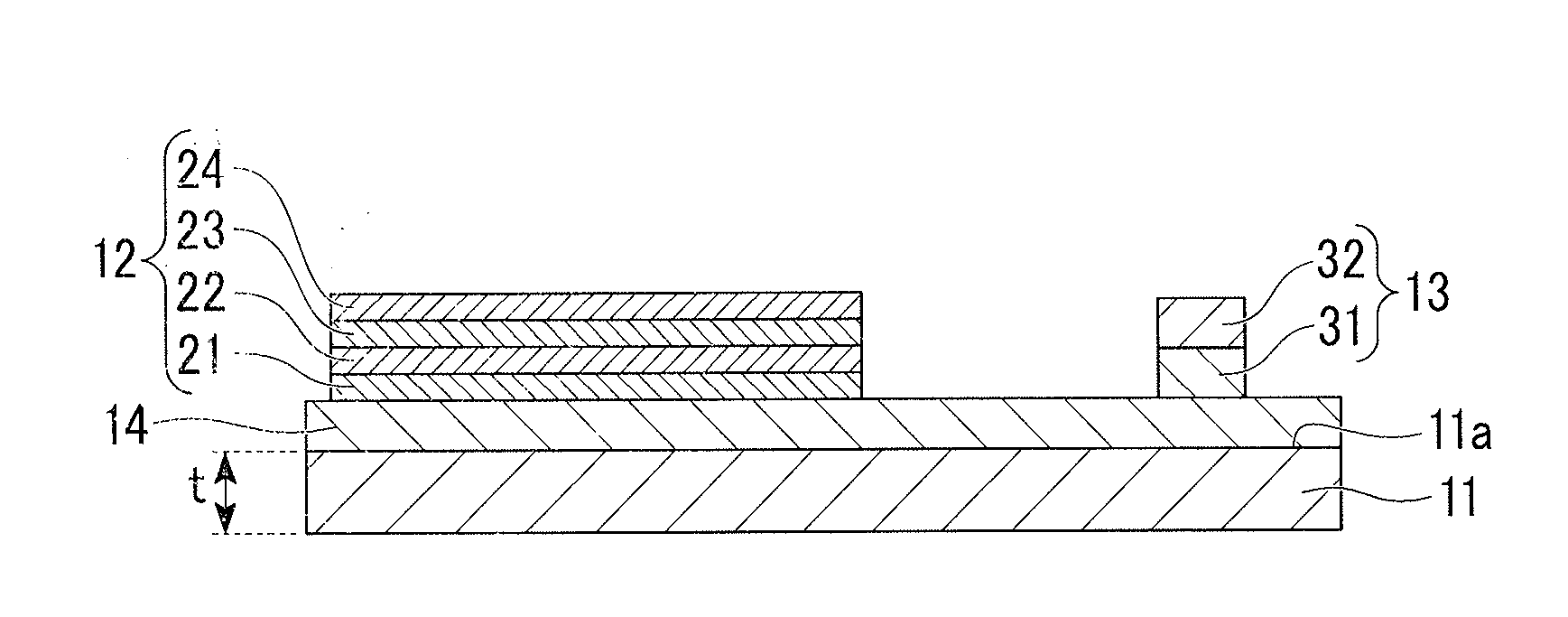
An AlN single crystal Schottky barrier diode including: an AlN single crystal substrate having a defect density of 106 cm−2 or less and a thickness of 300 μm or more; a first electrode formed on one surface of the AlN single crystal substrate; and a second electrode formed on one surface of the AlN single crystal substrate while being spaced apart from the first electrode, the AlN single crystal Schottky barrier diode being provided with: a rectifying property such that an on-off ratio at the time of applying 10 V and −40 V is at least 103 even at a high temperature of 573 K; a high voltage resistance such that a voltage can be applied at least within a range of −40 V to 10 V; and a low on-resistance characteristic such that a current begins to flow at no greater than 5 V.

Description

TECHNICAL FIELD[0001]The present invention relates to an AlN single crystal Schottky barrier diode and a method of producing the same.[0002]Priority is claimed on Japanese Patent Application No. 2012-016926, filed Jan. 30, 2012, the content of which is incorporated herein by reference.BACKGROUND ART[0003]In recent years, attempts have been made actively to improve the energy efficiency of the power elements such as a power diode. Examples of the power diodes include Schottky barrier diodes (SBD) for obtaining rectifying properties. Since the power elements made of silicon materials are approaching the theoretical limit, the search for other materials that are more suitable for the power elements has been actively conducted.[0004]It has been shown, in theory, that the semiconductor materials having a wide band gap and which were regarded conventionally as insulating materials are suitable as power elements (Non-Patent Document 1). Examples of the semiconductor materials having a wide...

Claims


Application Information

Patent Timeline
IPC IPC(8): H01L29/66H01L29/45H01L29/47H01L29/872
CPCH01L29/66212H01L29/475H01L29/452H01L29/872H01L29/2003
Inventor IROKAWA, YOSHIHIROSHIMAMURA, KIYOSHIGARCIA VILLORA, ENCARNACION ANTONIA
Owner NAT INST FOR MATERIALS SCI
Learn More