

Flash memory cell with capacitive coupling between a metal floating gate and a metal control gate
- Summary
- Abstract
- Description
- Claims
- Application Information
AI Technical Summary
Benefits of technology
Problems solved by technology
Method used
Image

Examples
Embodiment Construction
, and the Claims.
IV. BRIEF DESCRIPTION OF THE DRAWINGS
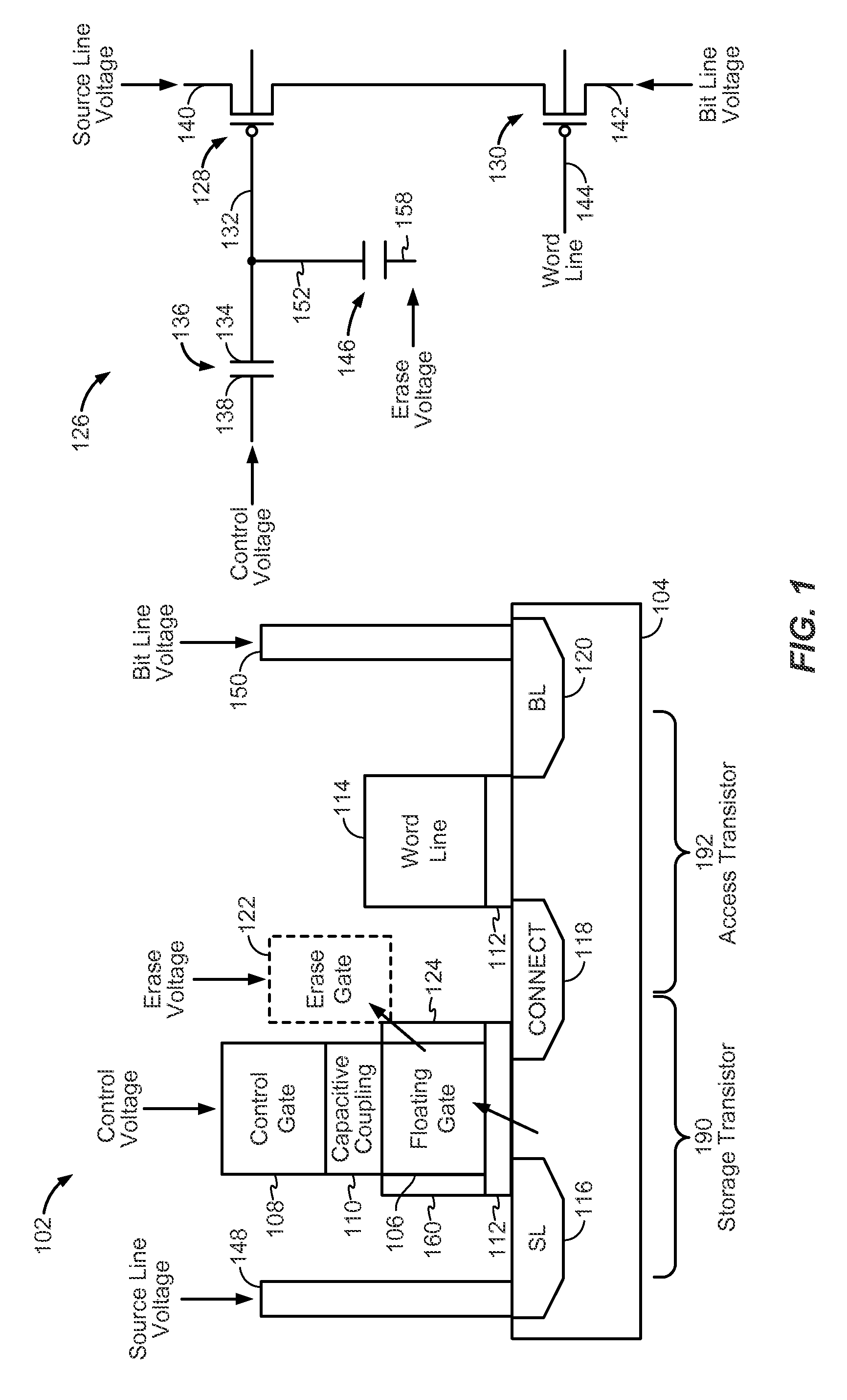
[0011]FIG. 1 is a diagram of a particular embodiment of a flash memory cell that is manufactured using a high-k / metal gate manufacturing process;
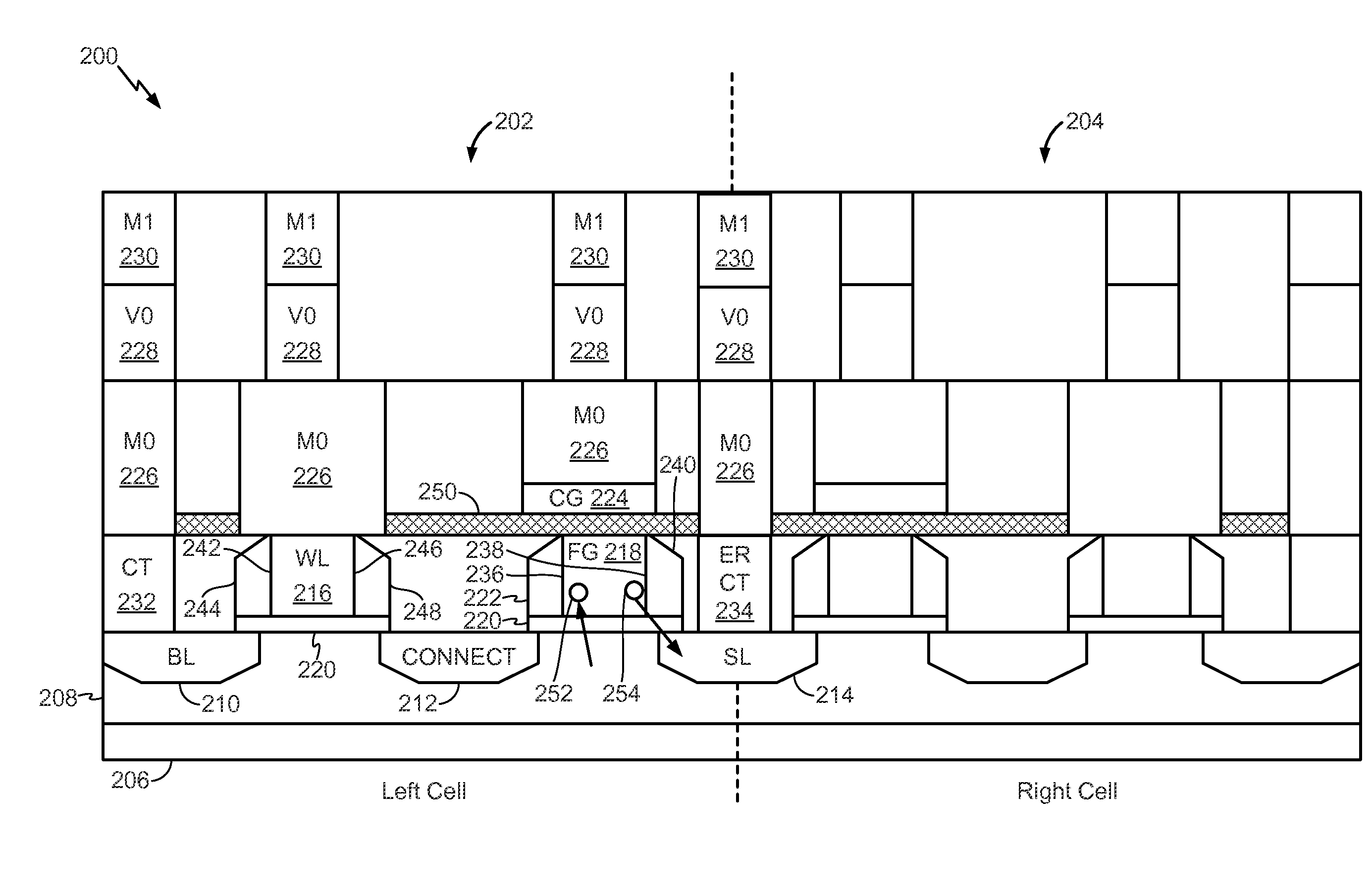
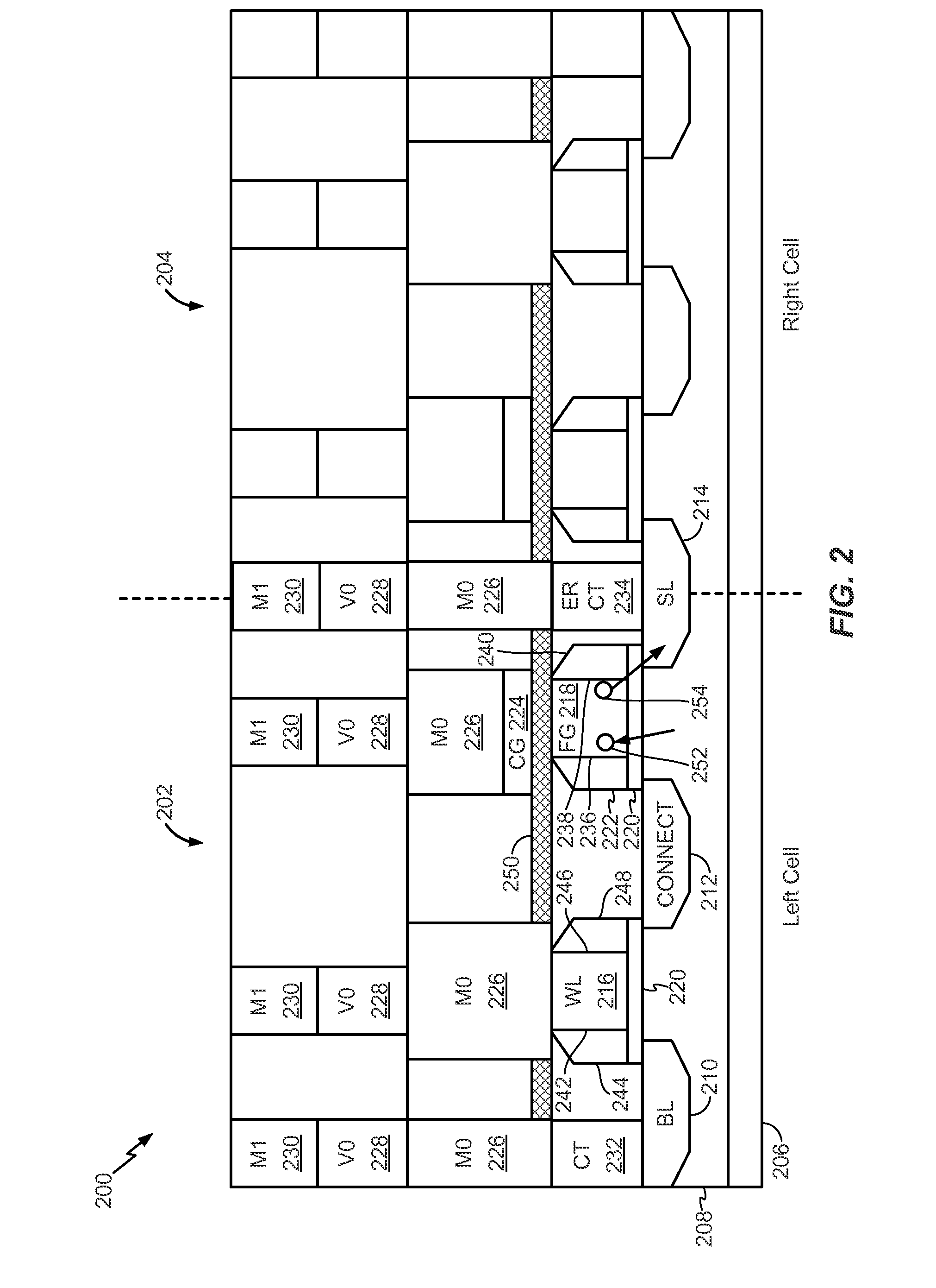
[0012]FIG. 2 is a cross section view of a particular embodiment of a flash memory cell array that includes a flash memory cell manufactured using a high-k / metal gate manufacturing process;
[0013]FIG. 3 is a cross section view of another particular embodiment of a flash memory cell array that includes a flash memory cell manufactured using a high-k / metal gate manufacturing process;
[0014]FIG. 4 is a cross section view of another particular embodiment of a flash memory cell array that includes a flash memory cell manufactured using a high-k / metal gate manufacturing process;
[0015]FIG. 5 is a cross section view of another particular embodiment of a flash memory cell array that includes a flash memory cell manufactured using a high-k / metal gate manufacturing process;
[0016]FIG. 6 is a cross sect...
PUM
 Abstract
Description
Claims
Application Information