Supercharge Your Innovation With Domain-Expert AI Agents!

Silicon wafer and method for manufacturing the same

Active Publication Date: 2015-02-12
GLOBALWAFERS JAPAN
View PDF2 Cites 2 Cited by
  • Summary
  • Abstract
  • Description
  • Claims
  • Application Information

AI Technical Summary

Benefits of technology

The present invention aims to provide a high-quality silicon wafer for use in the manufacturing of semiconductor devices. The silicon wafer should have fewer slip dislocations, defects, and oxygen precipitation nuclei, with the distribution of oxygen precipitation nuclei in the bulk portion being uniform with respect to the surface of the wafer. The invention also provides a method for manufacturing this high-quality silicon wafer.

Problems solved by technology

This reduces the pinning effect of oxygen during heat treatment in the later step of manufacturing a semiconductor device.
Thus, the higher the temperature of the heat treatment, the more likely slip dislocations are to occur.
However, if RTP is performed in an oxygen-containing gas atmosphere as disclosed in JP Patent Publication 2010-129918, especially if the RTP is performed at a temperature of less than 1300° C., there are the following two problems.
One is that since the oxygen concentration in the surface layer of the wafer has increased due to inward dispersion of oxygen, oxide films on the inner walls of COPs are less likely to melt, so that COPs cannot be easily removed.
Another problem is that since it is impossible to melt oxygen precipitation nuclei produced while crystals are growing, if the nuclei have ununiform density and size distributions in the radial direction of the surface of the wafer, these nuclei could grow into oxygen precipitates that are ununiform in density and size during the later heat treatment step, thus reducing the strength of the wafer.

Method used


Image

  • Silicon wafer and method for manufacturing the same
  • Silicon wafer and method for manufacturing the same

Examples


Embodiment Construction

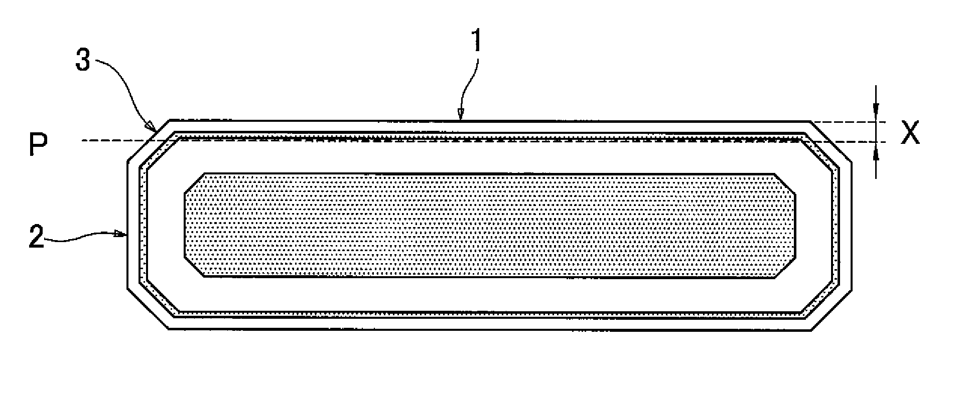
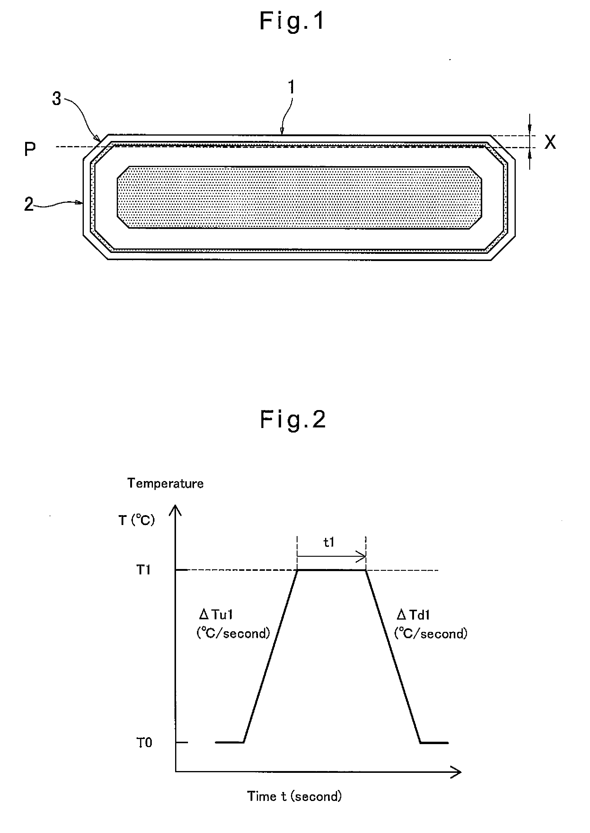
[0026]Now the present invention is described in a detailed manner. The method of manufacturing a silicon wafer according to the present invention includes the step of subjecting a silicon wafer sliced from a silicon single-crystal ingot grown by the Czochralski process to a predetermined RTP, and the below-described predetermined removal step. By performing the RTP and then the removal step, crystal defects decrease in the device region of the completed silicon wafer, and oxygen precipitation nuclei in the bulk portion of the completed silicon wafer are uniformly arranged in the radial direction of the surface of the wafer.

[0027]During the RTP, which is performed in an oxygen-containing atmosphere, the wafer is heated to a maximum temperature within a range of 1300 to 1380° C., and kept at the maximum temperature for 5 to 60 seconds. By performing such RTP, it is possible to effectively eliminate COPs and oxygen precipitation nuclei that have been produced during growth of the silic...


PUM

PropertyMeasurementUnit
Temperatureaaaaaaaaaa
Lengthaaaaaaaaaa

Abstract

A silicon wafer is manufactured by subjecting a silicon wafer sliced from a silicon single-crystal ingot grown by the Czochralski process to a rapid thermal process in which the silicon wafer is heated to a maximum temperature within a range of 1300 to 1380° C., and kept at the maximum temperature for 5 to 60 seconds; and removing a surface layer of the wafer where a semiconductor device is to be manufactured by a thickness of not less X [μm] which is calculated according to the below equations (1) to (3):X[μm]=a[μm]+b[μm]  (1);a[μm]=(0.0031×(said maximum temperature)[° C.]−3.1)×6.4×(cooling rate)−0.4[° C. / second] . . . (2); andb[μm]=a / (solid solubility limit of oxygen) [atoms / cm3] / (oxygen concentration in substrate) [atoms / cm3]  (3).

Description

CROSS REFERENCE TO RELATED APPLICATIONS[0001]This application is based on and claims priority under 35 U.S.C. sctn. 119 with respect to Japanese Patent Application No. 2013-163958 filed on Aug. 7, 2013, the entire content of which is incorporated herein by reference.BACKGROUND OF THE INVENTION[0002]This invention relates to a silicon wafer (hereinafter sometimes simply referred to as the “wafer”) suitable for use as a substrate on which a semiconductor device is to be manufactured, and a method for manufacturing such a wafer.[0003]For a silicon wafer for use as a substrate on which a semiconductor device is to be manufactured, it is required that its surface layer which is used as an active region where a semiconductor device is to be manufactured be free of defects by reducing e.g. crystal-originated particles (COPs) and laser scattering tomography defects (LSTDs).[0004]In order to improve productivity of such a silicon wafer, in a recently developed method, at least the surface of...

Claims


Application Information

Patent Timeline
IPC IPC(8): H01L29/16C30B29/06H01L21/02C30B33/02
CPCH01L29/16C30B33/02H01L21/02008H01L21/02013C30B29/06C30B15/206H01L21/3225H01L21/324Y10T428/24488Y10T428/31
Inventor ARAKI, KOJIAOKI, TATSUHIKOSUDO, HARUOSENDA, TAKESHI
Owner GLOBALWAFERS JAPAN
Features
  • R&D
  • Intellectual Property
  • Life Sciences
  • Materials
  • Tech Scout
  • Unparalleled Data Quality
  • Higher Quality Content
  • 60% Fewer Hallucinations
Learn More