Capacitor and Semiconductor Device

Active Publication Date: 2015-02-26
SEMICON ENERGY LAB CO LTD
View PDF6 Cites 21 Cited by
  • Summary
  • Abstract
  • Description
  • Claims
  • Application Information

AI Technical Summary

Benefits of technology

The present invention provides a method for forming an aluminum oxide film using atomic layer deposition. By alternating the introduction of trimethylaluminum and water vapor, the deposition time is lengthened, resulting in reduced throughput. However, the invention also provides a semiconductor device that includes a transistor with excellent electrical characteristics, a capacitor with increased capacitance and improved aperture ratio, and a semiconductor device with high yield and productivity. Furthermore, the invention can reduce the duration of the atomic layer deposition process, resulting in more efficient production.

Problems solved by technology

The transistor that is normally-on causes various problems that a malfunction is likely to be caused when the transistor is in operation and power consumption is increased when the transistor is not in operation, for example.
Furthermore, there is a problem in that the amount of change in electrical characteristics, typically in threshold voltage, of the transistor over time or due to a stress test is increased.
However, in the case where an aluminum oxide film is formed by a sputtering method using an aluminum oxide target, arcing is caused and thus fine particles are generated.
Entry of the fine particles into a deposited film leads to a reduction in yield.

Method used


Image

  • Capacitor and Semiconductor Device
  • Capacitor and Semiconductor Device
  • Capacitor and Semiconductor Device

Examples


embodiment 1

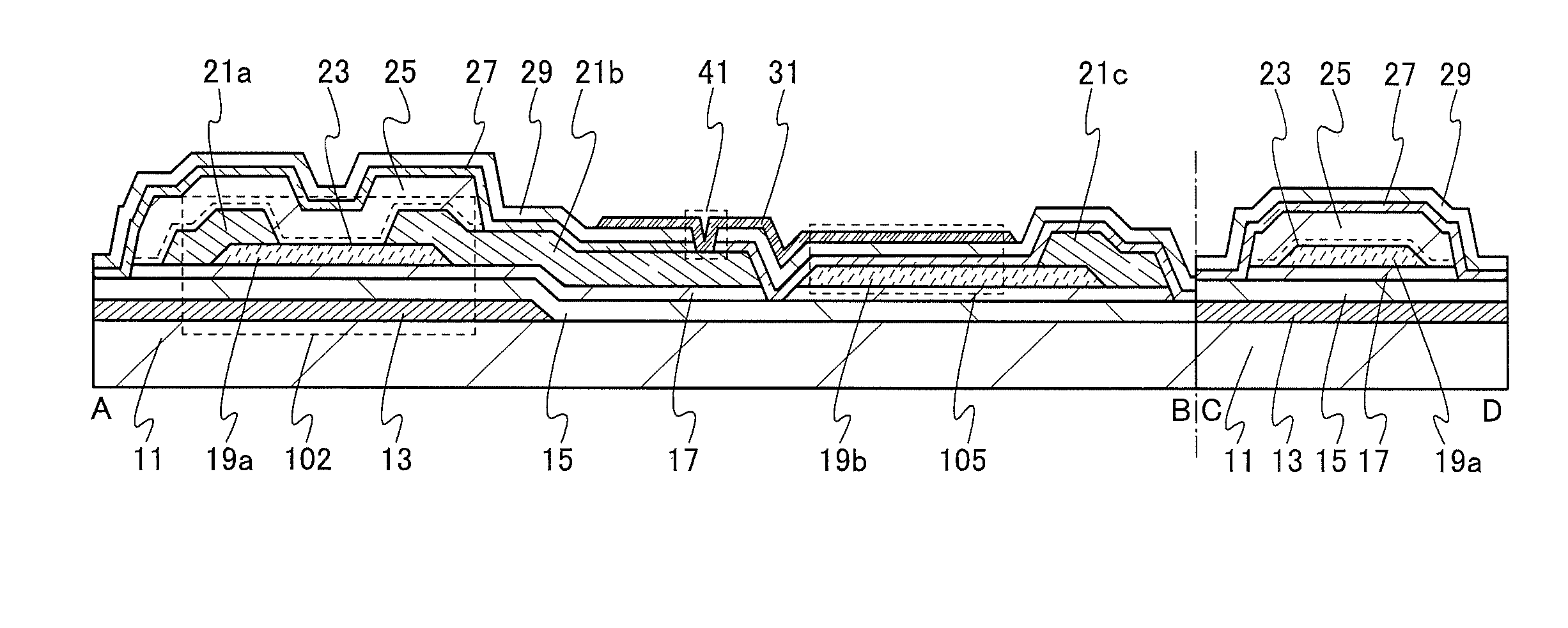
[0060]In this embodiment, a semiconductor device of one embodiment of the present invention will be described with reference to drawings. Note that in this embodiment, a semiconductor device of one embodiment of the present invention will be described taking a display device as an example. In addition, in this embodiment, an oxide semiconductor film will be described as a semiconductor film.

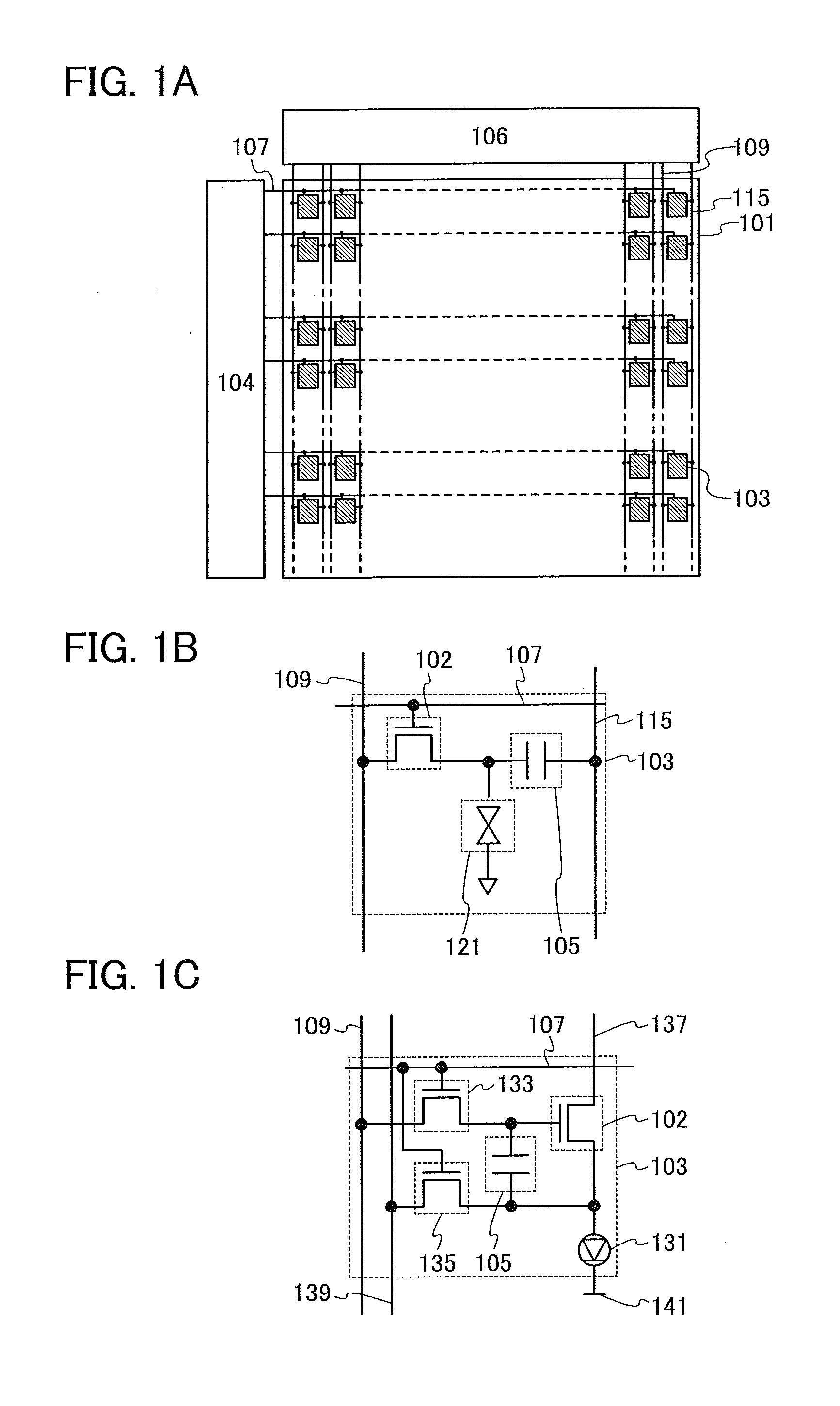
[0061]FIG. 1A illustrates an example of a semiconductor device. The semiconductor device illustrated in FIG. 1A includes a pixel portion 101, a scan line driver circuit 104, a signal line driver circuit 106, m scan lines 107 that are arranged parallel or substantially parallel to one another and whose potentials are controlled by the scan line driver circuit 104, and n signal lines 109 that are arranged parallel or substantially parallel to one another and whose potentials are controlled by the signal line driver circuit 106. The pixel portion 101 includes a plurality of pixels 103 arranged in a ...

modification example 1

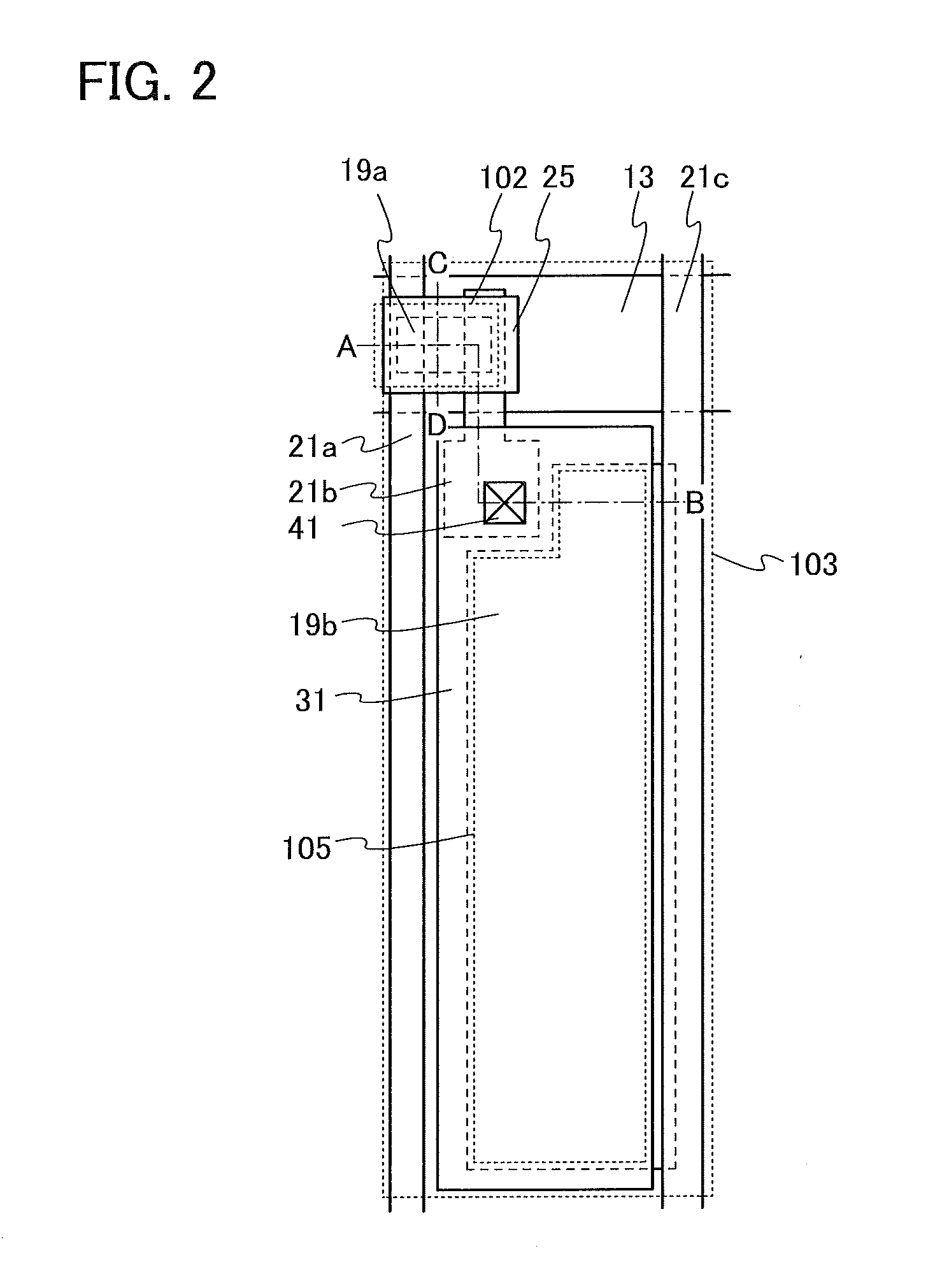
[0238]Here, modification examples of the metal oxide film 27 described in Embodiment 1 will be described with reference to FIGS. 8A and 8B.

[0239]FIGS. 8A and 8B are top views of the pixel 103. Components of the transistor 102 are shown by dotted lines and the metal oxide film 27 is hatched.

[0240]As illustrated in FIG. 8A, the metal oxide film 27 can be formed over an entire surface of the pixel 103, which can prevent oxygen contained in the oxide insulating film 23 or 25 from transferring to the outside. Consequently, oxygen vacancies in the oxide semiconductor film 19a can be reduced.

[0241]Alternatively, metal oxide films 27a and 27b, which are isolated from each other, may be formed in the pixel 103 as illustrated in FIG. 8B. By reducing the thickness of the metal film 26 formed in the step in FIG. 6A, the metal oxide films 27a and 27b can be formed. Alternatively, a metal oxide film may be formed over an entire surface of the pixel 103 and then part of the metal oxide film is rem...

modification example 2

[0245]FIG. 9 illustrates a modification example of the semiconductor device described in Embodiment 1.

[0246]The semiconductor device in FIG. 9 is different from the semiconductor device in FIG. 3 in the formation order of the metal oxide film 27 and the nitride insulating film 29. That is, the nitride insulating film 29 is formed over the nitride insulating film 15, the oxide insulating film 17, the film 19b having conductivity, the conductive films 21a and 21b serving as a pair of electrodes, the conductive film 21c, and the oxide insulating films 23 and 25, and the metal oxide film 27 is formed over the nitride insulating film 29. The conductive film 31 serving as a pixel electrode is formed over the metal oxide film 27.

[0247]In the semiconductor device in FIG. 9, the film 19b having conductivity included in the capacitor 105 is in contact with the nitride insulating film 29. The nitride insulating film 29 is provided between the film 19b having conductivity and the metal oxide fi...


PUM


Abstract

A semiconductor device has an insulating surface provided with a transistor and a capacitor. The transistor includes a gate electrode, an oxide semiconductor film overlapping with the gate electrode, a gate insulating film between the gate electrode and the oxide semiconductor film, and a first conductive film serving as a pair of electrodes in contact with the oxide semiconductor film. An oxide insulating film in contact with the oxide semiconductor film, a metal oxide film over the oxide insulating film, and a second conductive film serving as a pixel electrode which is in an opening in the metal oxide film and is in contact with the first conductive film are provided. The capacitor includes a film having conductivity over the gate insulating film, the second conductive film, and the metal oxide film provided between the film having conductivity and the second conductive film.

Description

BACKGROUND OF THE INVENTION[0001]1. Field of the Invention[0002]The present invention relates to an object, a method, or a manufacturing method. The present invention relates to a process, a machine, manufacture, or a composition of matter. One embodiment of the present invention particularly relates to a semiconductor device, a display device, a light-emitting device, a power storage device, a driving method thereof, or a manufacturing method thereof. In particular, one embodiment of the present invention relates to a capacitor including, as an electrode, a film containing materials that can form an oxide semiconductor and a manufacturing method thereof, or a semiconductor device including a transistor including an oxide semiconductor film and a manufacturing method thereof.[0003]2. Description of the Related Art[0004]Attention has been focused on a technique for forming a transistor using a semiconductor thin film formed over a substrate (also referred to as a thin film transistor...

Claims


Application Information

Patent Timeline
IPC IPC(8): H01L27/12H01L29/786H01L49/02
CPCH01L27/1255H01L29/7869H01L28/40H01L29/94H01L27/1225H01L29/78696
Inventor YAMAZAKI, SHUNPEIKOEZUKA, JUNICHIKATAYAMA, MASAHIROJINTYOU, MASAMI
Owner SEMICON ENERGY LAB CO LTD
Why Eureka
Try Eureka