

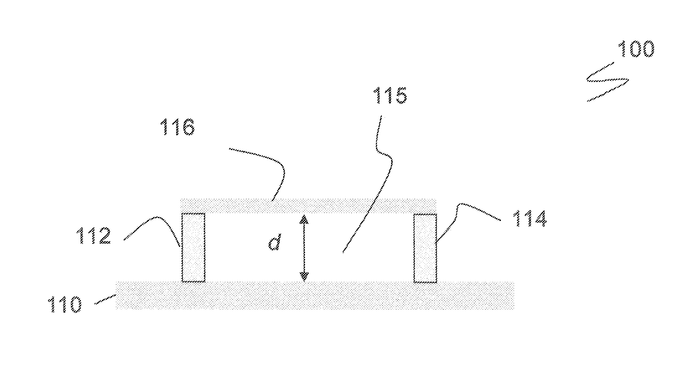
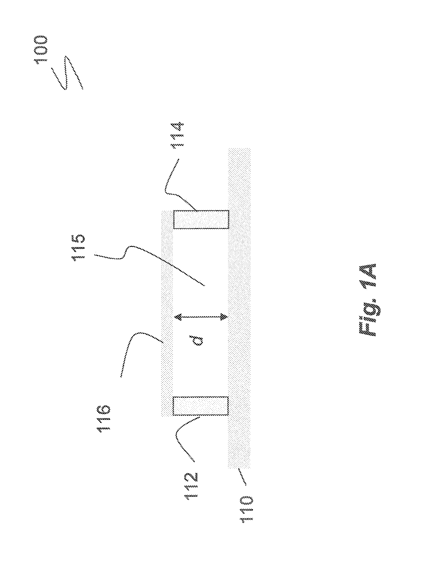
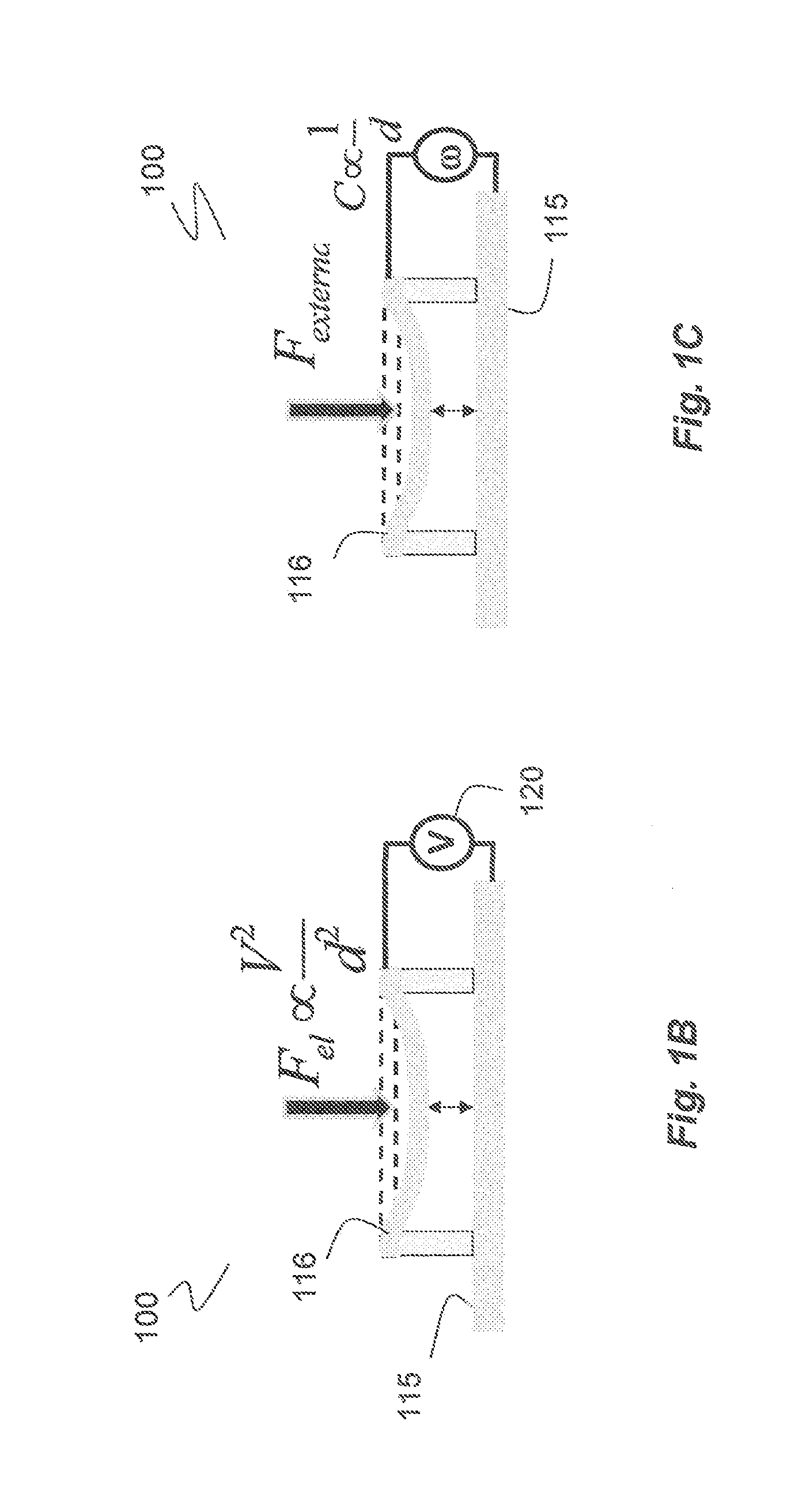
Method and apparatus for release-assisted microcontact printing of MEMS
a technology of microcontact printing and release-assisted microcontact, which is applied in the direction of fluid pressure measurement, fluid pressure measurement by electric/magnetic elements, instruments, etc., can solve the problems of limited size and form factor, limited material set, and limited conventional methods working within the existing silicon semiconductor-based framework
- Summary
- Abstract
- Description
- Claims
- Application Information
AI Technical Summary
Benefits of technology
Problems solved by technology
Method used
Image

Examples
example 1
[0060]A MEMS device was fabricated on patterned-silicon-dioxide-on-silicon substrate (SiO2 on Si) using contact-transfer stamping process outlined above. The fabrication steps comprised forming a transparency mask, forming the master mold, forming pick-up stamp substrates, forming transfer pad with raised mesas and contact-transfer of the mesa diaphragm onto the MEMS structure.
[0061]Photolithography Transparency Masks—The first step in fabricating the diaphragm involves making the transparency masks that define the desired geometry. The masks can be used in ultraviolet (UV) photolithography for patterning photoresists. UV photolithography was used for making SU-8 masters that were then used as molds for patterning the PDMS transfer pad. EPON SU-8 (MicroChem Corp.®; SU-8 3010) is a commonly used epoxy-based photoresist. The portion of SU-8 resist that is exposed to light becomes insoluble to the SU-8 photoresist developer, propylene glycol monomethyl ether acetate (PGMEA), while the ...
PUM
| Property | Measurement | Unit |
|---|---|---|
| surface area | aaaaa | aaaaa |
| surface area | aaaaa | aaaaa |
| area | aaaaa | aaaaa |
Abstract
Description
Claims
Application Information