Pattern forming method, actinic ray-sensitive or radiation-sensitive resin composition, resist film, manufacturing method of electronic device, and electronic device

Active Publication Date: 2015-03-19
FUJIFILM CORP
View PDF16 Cites 7 Cited by
  • Summary
  • Abstract
  • Description
  • Claims
  • Application Information

AI Technical Summary

Benefits of technology

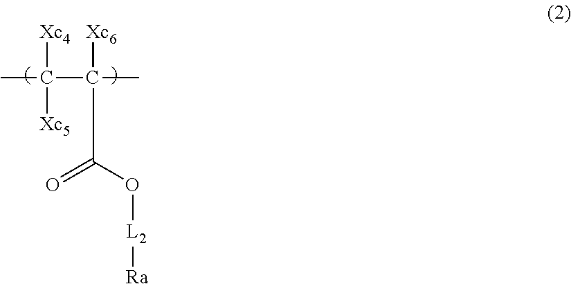
[0163]The specific examples of the repeating units having an acid group are shown below, but the invention is not restricted thereto.
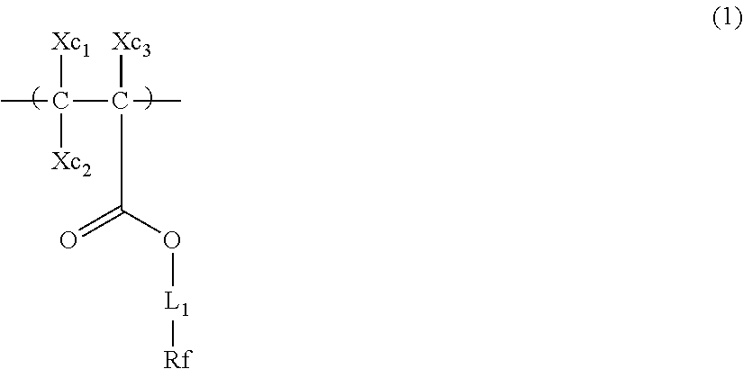
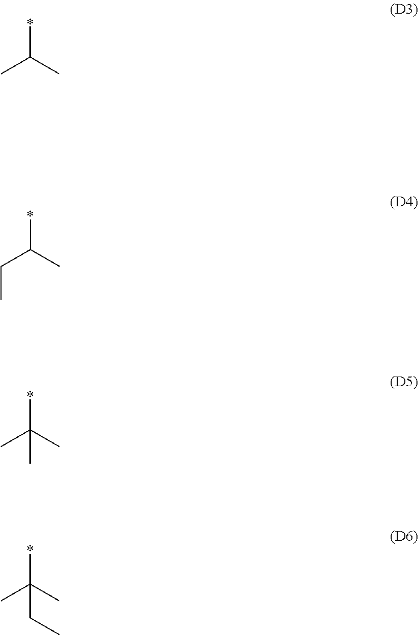
[0415]The specific examples of the repeating units having a CF3 partial structure are shown below, but the invention is not restricted thereto.
[0416]When the resin (D) contains a repeating unit having a CF3 partial structure, the content thereof is preferably 10 mol % or less, more preferably 8 mol % or less, and still more preferably 5 mol % or less, based on all the repeating units in the resin (D). Ideally, the resin (D) does not contain a CF3 partial structure.
[0417]The resin (D) may contain a repeating unit havin

Problems solved by technology

However, in the above positive image-forming method, an isolated line or a dot pattern can be successfully formed, b

Method used


Image

  • Pattern forming method, actinic ray-sensitive or radiation-sensitive resin composition, resist film, manufacturing method of electronic device, and electronic device
  • Pattern forming method, actinic ray-sensitive or radiation-sensitive resin composition, resist film, manufacturing method of electronic device, and electronic device
  • Pattern forming method, actinic ray-sensitive or radiation-sensitive resin composition, resist film, manufacturing method of electronic device, and electronic device

Examples


Example

Synthesis Example

Synthesis of Resin A-1

[0690]Cyclohexanone (22.11 parts by mass) was heated to 80° C. under nitrogen flow. While stirring the solution, a mixed solution containing 5.69 parts by mass of the monomer represented by the following formula M-1, 5.46 parts by mass of the monomer represented by the following formula M-2, 41.07 parts by mass of cyclohexanone, and 0.59 parts by mass of dimethyl-2,2′-azobisisobutyrate (V-601, manufactured by Wako Pure Chemical Industries) was dropwise added over 4 hours. After completion of dropping, the solution was further stirred for 2 hours at 80° C. After being allowed to be cooled, the reaction solution was reprecipitated by hexane / ethyl acetate (mass ratio: 9 / 1), filtered, and the obtained solid was subjected to vacuum drying to thereby obtain 8.85 parts by mass of resin (A-1) of the invention.

[0691]The weight average molecular weight (Mw: in terms of polystyrene) of the obtained resin found by GPC (carrier: tetrahydrofuran (THF)) was M...

Example

Examples 1 to 26 and Comparative Examples 1 and 2

ArF Immersion Exposure

(Preparation of Resist)

[0708]The components shown in the following table were dissolved in the solvent shown in the same table to give a solid content of 5.0 mass %, and the obtained solution is filtered through a polyethylene filter having a pore size of 0.03 μm to prepare an actinic ray-sensitive or radiation-sensitive resin composition (resist composition). An organic antireflection film, ARC29SR (manufactured by Nissan Chemical Industries, Ltd.), was coated on a silicon wafer and baked at 205° C. for 60 seconds to form an antireflection film having a thickness of 0110 nm, and the actinic ray-sensitive or radiation-sensitive resin composition was coated thereon and baked (PB: Prebake) at 90° C. for 60 seconds to form a resist film having a thickness of 120 nm.

[0709]The obtained wafer was subjected to pattern exposure by using an ArF excimer laser immersion scanner (XT1700i, manufactured by ASML, NA: 1.20, C-Qu...

Example

[0716]By using the resist in Example 1 and referring to U.S. Pat. No. 8,227,183B, Example 7 and the like, line and space mask pattern was exposed and then performed both alkali development and butyl acetate development. In this evaluation, pattern of the pitch of ½ of mask pattern was able to be formed.

[0717]Also, in Example 1, evaluation was performed similarly except for adding a small amount of tri-n-octylamine to the developer (butyl acetate). Also good pattern forming was able to be conducted.

[0718]A composition was prepared and evaluated in the same manner as in Examples 24 and 25 except for changing compound N-13 to Compound Cl-1, Compound Cl-7, respectively. It was confirmed that the obtained resist performance was almost the same level as in Examples 24 and 25.

INDUSTRIAL APPLICABILITY

[0719]According to the invention, a pattern forming method excellent in reduction of bridge defect and restrained in generation of particles in pattern formation of a fine pattern having a line...


PUM

PropertyMeasurementUnit
Fractionaaaaaaaaaa
Massaaaaaaaaaa
Structureaaaaaaaaaa

Abstract

There is provided a pattern forming method comprising (i) a step of forming a film by an actinic ray-sensitive or radiation-sensitive resin composition; (ii) a step of exposing the film; and (iii) a step of performing development by using a developer containing an organic solvent to form a negative pattern, wherein the actinic ray-sensitive or radiation-sensitive resin composition contains (A) a resin capable of increasing the polarity by an action of an acid to decrease the solubility in a developer containing an organic solvent, (B) a compound capable of generating an acid upon irradiation with an actinic ray or radiation, (C) a solvent, and (D) a resin having a repeating unit having a fluorine atom and not having a CF3 partial structure.

Description

CROSS REFERENCE TO RELATED APPLICATION[0001]This is a continuation of International Application No. PCT / JP2013 / 064967 filed on May 23, 2013, and claims priority from Japanese Patent Application No. 2012-118056 filed on May 23, 2012, U.S. Provisional Application No. 61 / 650,710 filed on May 23, 2012, and Japanese Patent Application No. 2013-046376 filed on Mar. 8, 2013 the entire disclosures of which are incorporated therein by reference.TECHNICAL FIELD[0002]The present invention relates to a pattern forming method, an actinic ray-sensitive or radiation-sensitive resin composition, a resist film, a manufacturing method of an electronic device, and an electronic device. More specifically, the present invention relates to a pattern forming method suitably used for lithographic processes in the manufacture of a semiconductor such as IC, the manufacture of a liquid crystal device and a circuit board such as a thermal head, and further other photo-fabrication, an actinic ray-sensitive or r...

Claims


Application Information

Patent Timeline
IPC IPC(8): G03F7/038G03F7/30
CPCG03F7/0388G03F7/30G03F7/038G03F7/0397G03F7/091G03F7/11G03F7/2041G03F7/325G03F7/40G03F7/0046C08F220/1807C08F220/1818C08F220/1804C08F220/1806C08F220/1803C08F220/1805C08F220/1808C08F220/1811C08F220/22G03F7/32C08F220/18C08F220/283C08F220/281H01L21/0273G03F7/004G03F7/039H01L21/027
Inventor ITO, JUNICHIYAMAGUCHI, SHUHEITAKAHASHI, HIDENORIYAMAMOTO, KEI
Owner FUJIFILM CORP
Why Eureka
Try Eureka