Method for stabilizing an interface post etch to minimize queue time issues before next processing step

a technology of queue time and interface, which is applied in the direction of semiconductor devices, electrical equipment, electric discharge tubes, etc., can solve the problems of inoperable circuit, undesirable metal diffusion into the dielectric bulk insulating material, and degrade the overall performance of the integrated circui

Inactive Publication Date: 2015-03-19
APPLIED MATERIALS INC
View PDF9 Cites 19 Cited by
  • Summary
  • Abstract
  • Description
  • Claims
  • Application Information

AI Technical Summary

Problems solved by technology

Reliably producing sub-half micron and smaller features is one of the key technology challenges for next generation very large scale integration (VLSI) and ultra large-scale integration (ULSI) of semiconductor devices.
However, as the limits of circuit technology are pushed, the shrinking dimensions of VLSI and ULSI interconnect technology have placed additional demands on processing capabilities.
Capacitive coupling between adjacent metal interconnects may cause cross talk and / or resistance-capacitance (RC) delay which degrades the overall performance of the integrated circuit and may render the circuit inoperable.
Diffusion of the metal into the dielectric bulk insulating material is undesirable because such diffusion can affect the electrical performance of the integrated circuit, or render the circuit inoperative.
Excess native oxide accumulation or contaminants may adversely affect the nucleation capability of the metal elements to adhere to the substrate surface during a subsequently metallization process.
Furthermore, poor adhesion at the interface may also result in undesired high contact resistance, thereby resulting in undesirably poor electrical properties of the device.
In addition, poor nucleation of the metal elements in the back end interconnection may impact not only the electrical performance of the devices, but also on the integration of the conductive contact material subsequently formed thereon.

Method used


Image

  • Method for stabilizing an interface post etch to minimize queue time issues before next processing step
  • Method for stabilizing an interface post etch to minimize queue time issues before next processing step
  • Method for stabilizing an interface post etch to minimize queue time issues before next processing step

Examples


Embodiment Construction

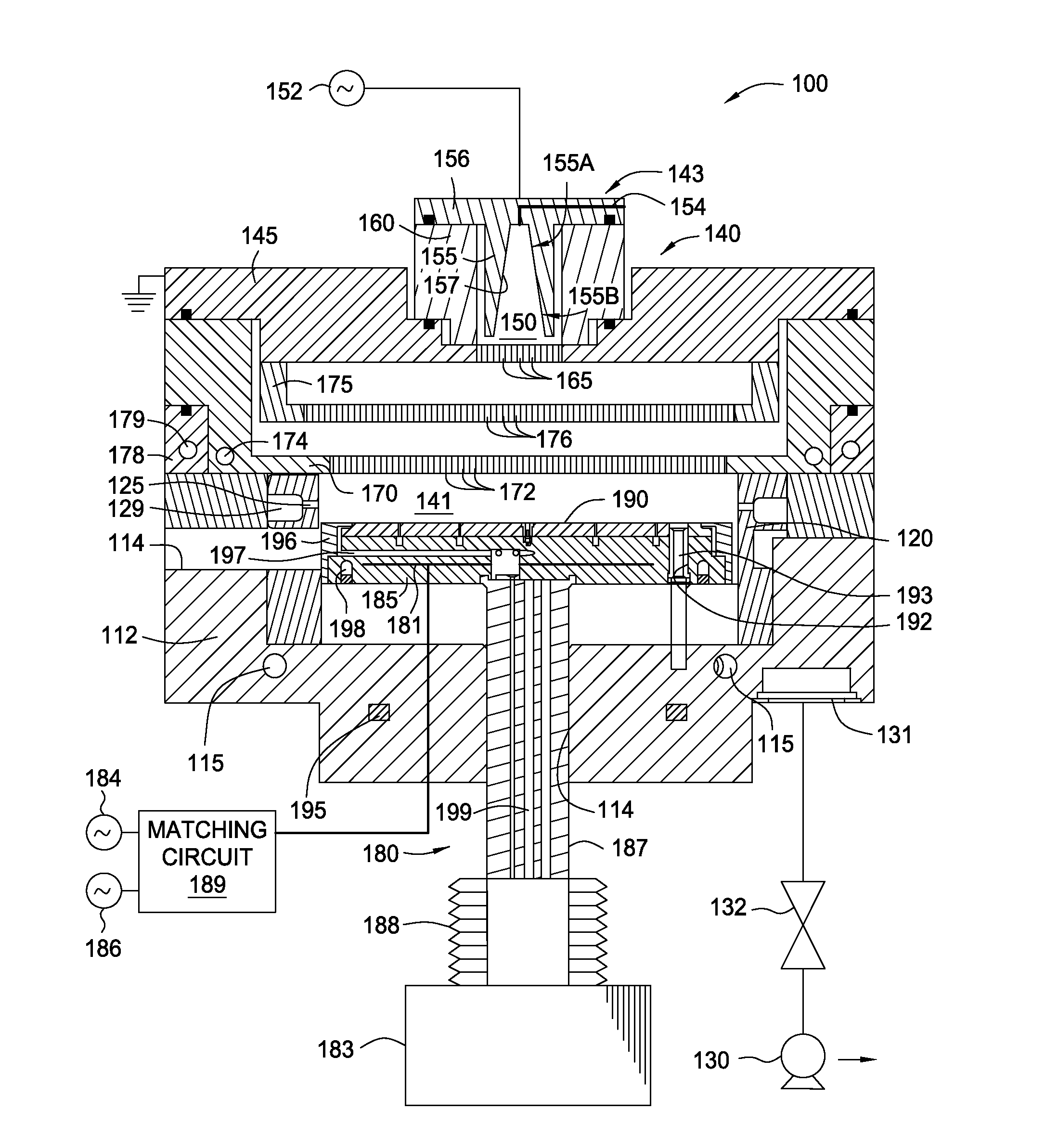
[0021]Methods for etching a dielectric barrier layer followed by an interface protection layer deposition process are disclosed herein which provide an etching process with high etching selectivity and interface protection after the etching process. In one embodiment, the dielectric barrier layer etching process includes using a low temperature etching process to selectively etching the dielectric barrier layer without over-etching to an underlying conductive layer. An interface protection layer is subsequently performed to protect the underlying conductive layer exposed after the dielectric barrier layer etching process. By utilizing an etching process with high etching selectivity along with the deposition of an interface protection layer after etching, a good interface control may be obtained. Additionally, Q-time control prior to performing a subsequent process may be extended with minimum oxide or contamination generation, thereby increasing manufacturing flexibility without de...


PUM

PropertyMeasurementUnit
temperatureaaaaaaaaaa
RF bias poweraaaaaaaaaa
temperatureaaaaaaaaaa

Abstract

Methods for etching a dielectric barrier layer disposed on the substrate using a low temperature etching process along with a subsequent interface protection layer deposition process are provided. In one embodiment, a method for etching a dielectric barrier layer disposed on a substrate includes transferring a substrate having a dielectric barrier layer disposed thereon into an etching processing chamber, performing a treatment process on the dielectric barrier layer, remotely generating a plasma in an etching gas mixture supplied into the etching processing chamber to etch the treated dielectric barrier layer disposed on the substrate, plasma annealing the dielectric barrier layer to remove the dielectric barrier layer from the substrate, and forming an interface protection layer after the dielectric barrier is removed from the substrate.

Description

BACKGROUND OF THE INVENTION[0001]1. Field of the Invention[0002]Embodiments of the present invention generally relate to methods for forming semiconductor devices. More particularly, embodiments of the present invention generally relate to methods for etching a dielectric barrier layer followed by an interface protection layer deposition process for manufacturing semiconductor devices.[0003]2. Description of the Related Art[0004]Reliably producing sub-half micron and smaller features is one of the key technology challenges for next generation very large scale integration (VLSI) and ultra large-scale integration (ULSI) of semiconductor devices. However, as the limits of circuit technology are pushed, the shrinking dimensions of VLSI and ULSI interconnect technology have placed additional demands on processing capabilities. Reliable formation of gate structures on the substrate is important to VLSI and ULSI success and to the continued effort to increase circuit density and quality of...

Claims


Application Information

Patent Timeline
Patent Type & Authority Applications(United States)
IPC IPC(8): H01L21/3065
CPCH01L21/3065H01J37/32082H01J37/32357H01J37/32449H01J2237/334H01L21/02164H01L21/02274H01L21/31116H01L21/76807H01L21/76814H01L21/76826H01L21/76829H01L2221/1063
Inventor NEMANI, SRINIVAS D.GOPALRAJA, PRABURAMKOSHIZAWA, TAKEHITO
Owner APPLIED MATERIALS INC
Why Eureka
Try Eureka