Semiconductor device

a semiconductor and device technology, applied in the field of semiconductor devices, can solve the problems of low crystallinity of oxide semiconductor films, defects at the interface between stacked oxide semiconductor films, oxygen vacancies and dangling bonds, etc., to improve the electrical characteristics improve the reliability of a semiconductor device, and reduce the density of defect states

Inactive Publication Date: 2015-03-26
SEMICON ENERGY LAB CO LTD
View PDF4 Cites 21 Cited by
  • Summary
  • Abstract
  • Description
  • Claims
  • Application Information

AI Technical Summary

Benefits of technology

[0023]One embodiment of the present invention makes it possible to form an oxide semiconductor film with a low density of defect states. One embodiment of the present invention makes it possible to form an oxide semiconductor film with a low impurity concentration. One embodiment of the present invention makes it possible to improve electrical cha

Problems solved by technology

An oxide semiconductor film with low crystallinity is likely to include defects such as oxygen vacancies and dangling bonds.
In the case where stacked oxide semiconductor films formed using sputtering targets with different compositions have different crystallinities, defects are generated at the interface between the stacked oxide semiconductor films.
Defects included in an oxide semiconductor film or defects combined with hydrogen or the like might cause ca

Method used


Image

  • Semiconductor device
  • Semiconductor device
  • Semiconductor device

Examples


embodiment 1

[0075]In this embodiment, a semiconductor device of one embodiment of the present invention and a method for manufacturing the semiconductor device will be described with reference to drawings.

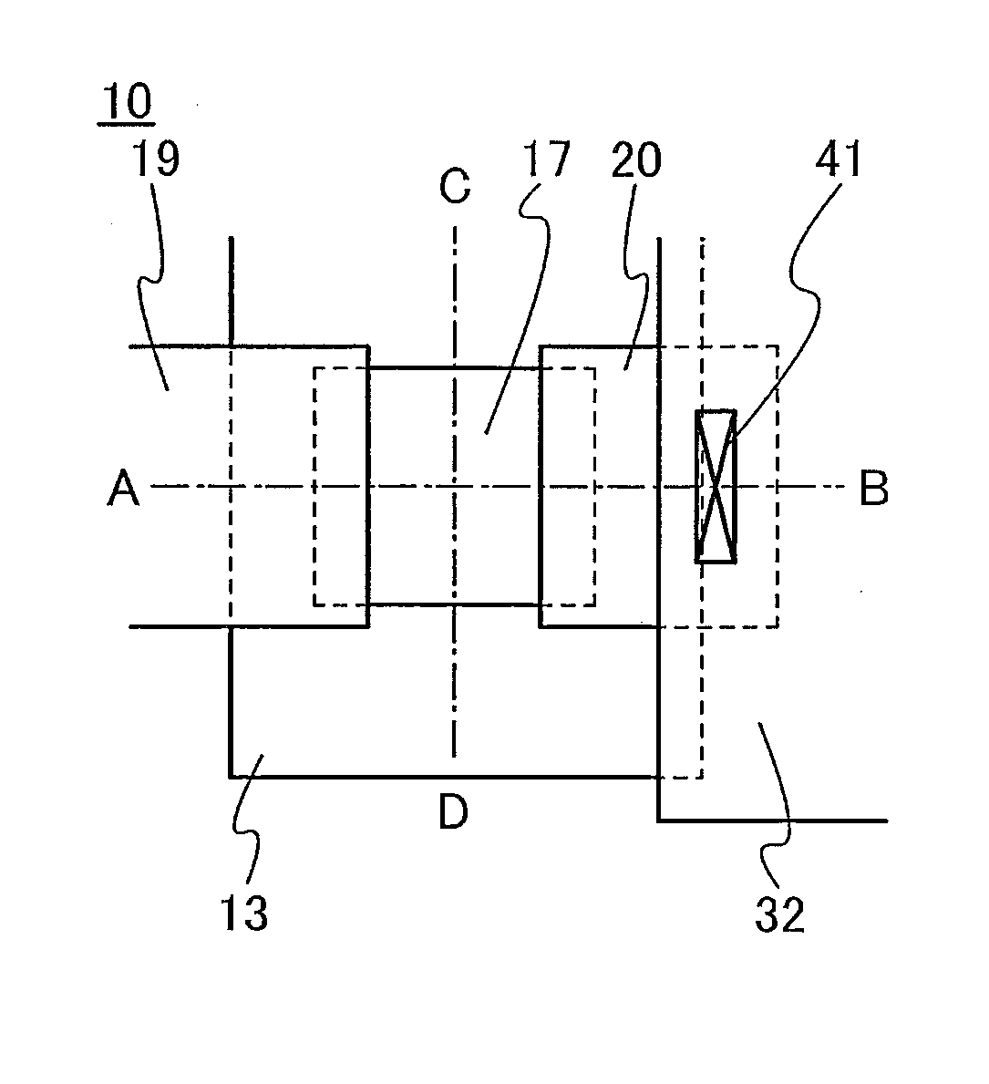
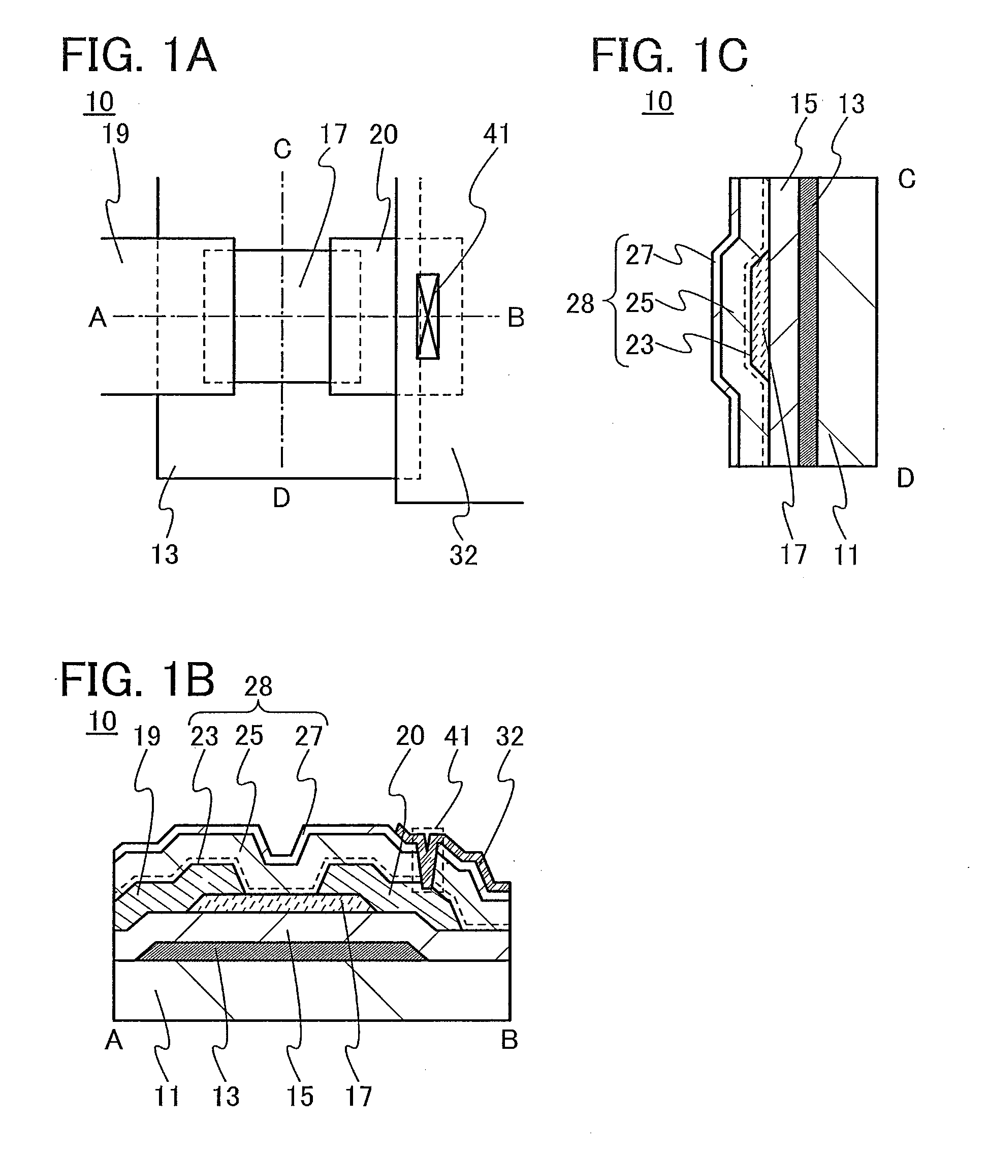
[0076]FIGS. 1A to 1C are a top view and cross-sectional views of a transistor 10 included in a semiconductor device. FIG. 1A is a top view of the transistor 10, FIG. 1B is a cross-sectional view taken along dashed-dotted line A-B in FIG. 1A, and FIG. 1C is a cross-sectional view taken along dashed-dotted line C-D in FIG. 1A. Note that in FIG. 1A, a substrate 11, a gate insulating film 15, an oxide insulating film 23, an oxide insulating film 25, a nitride insulating film 27, and the like are omitted for simplicity.

[0077]The transistor 10 illustrated in FIGS. 1B and 1C is a channel-etched transistor including a gate electrode 13 provided over the substrate 11; the gate insulating film 15 formed over the substrate 11 and the gate electrode 13; an oxide semiconductor film 17 overlapping with the ...

embodiment 2

[0279]In this embodiment, a semiconductor device of one embodiment of the present invention and a method for manufacturing the semiconductor device will be described with reference to drawings. Note that a transistor in this embodiment is different from that in Embodiment 1 in that two gate electrodes are included with an oxide semiconductor film provided therebetween.

[0280]FIGS. 9A to 9C are a top view and cross-sectional views of a transistor 40 included in a semiconductor device. FIG. 9A is a top view of the transistor 40, FIG. 9B is a cross-sectional view taken along dashed line A-B in FIG. 9A, and FIG. 9C is a cross-sectional view taken along dashed line C-D in FIG. 9A. Note that in FIG. 9A, the substrate 11, the gate insulating film 15, the oxide insulating film 23, the oxide insulating film 25, the nitride insulating film 27, and the like are omitted for simplicity.

[0281]The transistor 40 illustrated in FIGS. 9B and 9C is a channel-etched transistor including the gate electro...

modification example 3

[0325]A transistor having a structure different from those in FIGS. 1A to 1C, FIGS. 9A to 9C, FIGS. 11A to 11C, and FIGS. 12A to 12C will be described with reference to FIGS. 13A to 13C. In a transistor 80 illustrated in FIGS. 13A to 13C, the electrode 92 connected to one of the pair of electrodes 19 and 20 is provided over the nitride insulating film 87. Unlike the other transistors described in Embodiments 1 and 2, the transistor 80 includes an oxide insulating film 83 and an oxide insulating film 85, which are each separated for each transistor, over the oxide semiconductor film 17 and the pair of electrodes 19 and 20.

[0326]FIGS. 13A to 13C are a top view and cross-sectional views of the transistor 80 included in a semiconductor device. FIG. 13A is a top view of the transistor 80, FIG. 13B is a cross-sectional view taken along dashed-dotted line A-B in FIG. 13A, and FIG. 13C is a cross-sectional view taken along dashed-dotted line C-D in FIG. 13A. Note that in FIG. 13A, the subst...


PUM


Abstract

An oxide semiconductor film with a low density of defect states is formed. In addition, an oxide semiconductor film with a low impurity concentration is formed. Electrical characteristics of a semiconductor device or the like using an oxide semiconductor film is improved. A semiconductor device including a capacitor, a resistor, or a transistor having a metal oxide film that includes a region; with a transmission electron diffraction measurement apparatus, a diffraction pattern with luminescent spots indicating alignment is observed in 70% or more and less than 100% of the region when an observation area is changed one-dimensionally within a range of 300 nm.

Description

BACKGROUND OF THE INVENTION[0001]1. Field of the Invention[0002]The present invention relates to an object, a method, or a manufacturing method. In addition, the present invention relates to a process, a machine, manufacture, or a composition of matter. In particular, one embodiment of the present invention relates to a semiconductor device, a display device, a light-emitting device, a power storage device, a memory device, a driving method thereof, or a manufacturing method thereof. The present invention relates to a semiconductor device including a capacitor, a resistor, or a transistor that has an oxide semiconductor film and a manufacturing method thereof.[0003]2. Description of the Related Art[0004]Transistors used for most flat panel displays typified by a liquid crystal display device or a light-emitting display device include a silicon semiconductor such as amorphous silicon, single crystal silicon, or polycrystalline silicon formed over a glass substrate. A transistor using...

Claims


Application Information

Patent Timeline
IPC IPC(8): H01L27/12
CPCH01L27/1255H01L27/1229H01L27/1225H01L27/1222H01L29/7869
Inventor YAMAZAKI, SHUNPEIKOEZUKA, JUNICHIOKAZAKI, KENICHIHOSAKA, YASUHARU
Owner SEMICON ENERGY LAB CO LTD
Why Eureka
Try Eureka