Organic light emitting diode display panel and organic light emitting diode display device containing the same

a technology of light-emitting diodes and display panels, which is applied in the direction of thermoelectric device junction materials, semiconductor devices, electrical apparatus, etc., can solve the problems of reducing the yield rate of oled display devices, and achieve the reduction of the area of the non-display region, the density of the disposition of the spacer is increased, and the frictional force is larger.

Active Publication Date: 2015-04-02
INNOLUX CORP
View PDF1 Cites 23 Cited by
  • Summary
  • Abstract
  • Description
  • Claims
  • Application Information

AI Technical Summary

Benefits of technology

[0017]In addition, in the OLED display panels of both aforementioned aspects of the present invention, a distance between two adjacent spacers in the display region may be different from that in the non-display region. Preferably, the distance between two adjacent spacers in the display region is larger than that in the non-display region. Hence, when the first substrate and the second substrate are assembled with the frit sealant, the increased disposition density of the spacers in the non-display region can provide larger frictional force to prevent the shift between the first substrate and the second substrate. Furthermore, sizes of the spacers in the display region may also be different from those in the non-display region. Preferably, the sizes of the spacers in the display region are larger than those in the non-display region. Alternatively, projected areas of the projections of the spacers may be different from each other. Preferably, the projected areas thereof in the display region are larger than those in the non-display region. Since the spacers in the non-display region have smaller sizes or projected areas, the ar...

Problems solved by technology

However, during the laser heating process, a shift between the top substrate and the bottom substrate ...

Method used


Image

  • Organic light emitting diode display panel and organic light emitting diode display device containing the same
  • Organic light emitting diode display panel and organic light emitting diode display device containing the same
  • Organic light emitting diode display panel and organic light emitting diode display device containing the same

Examples


embodiment 1

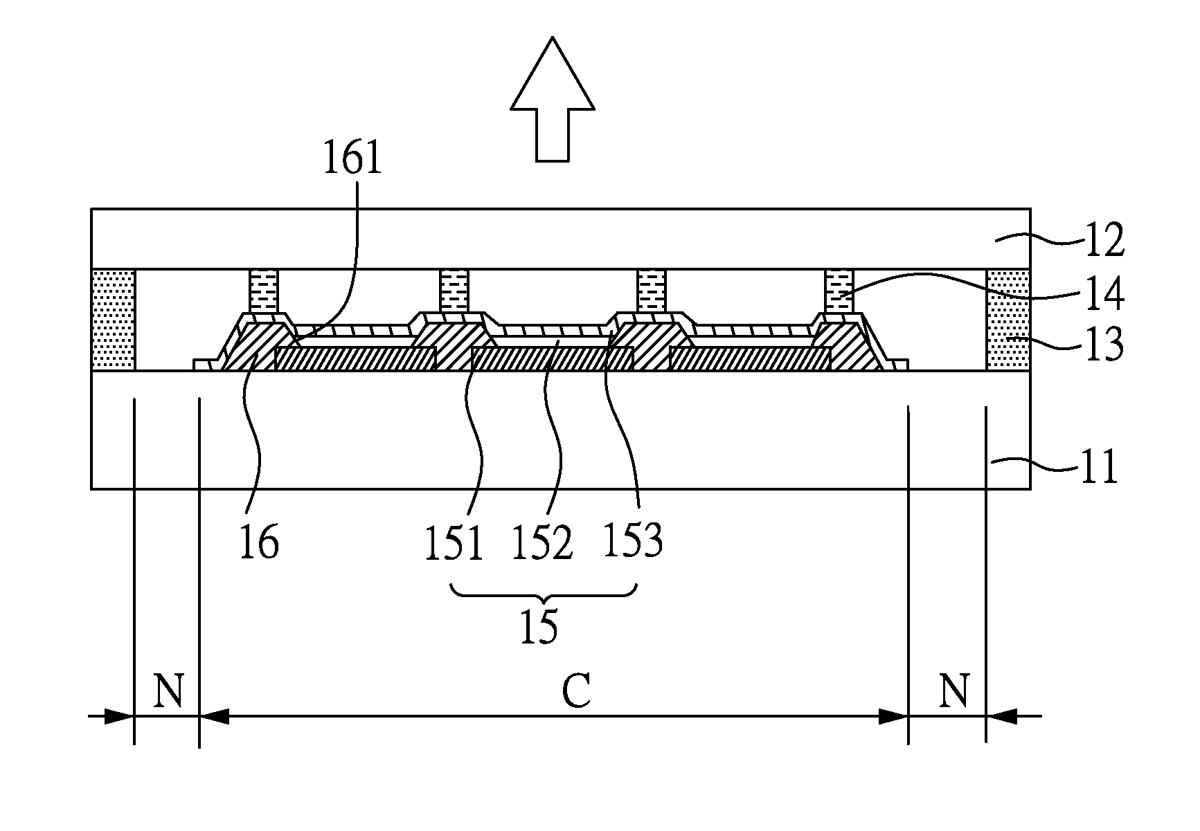
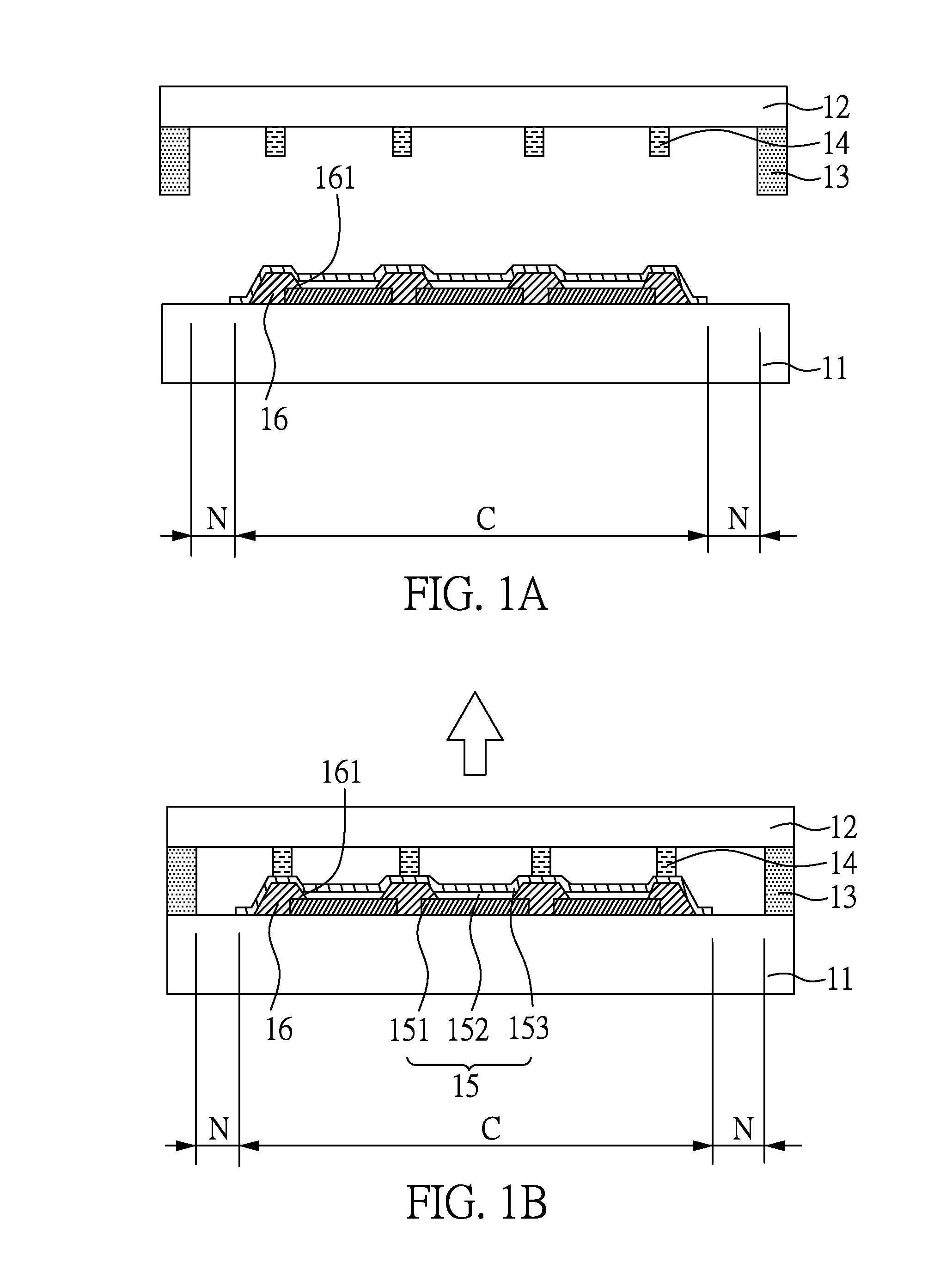
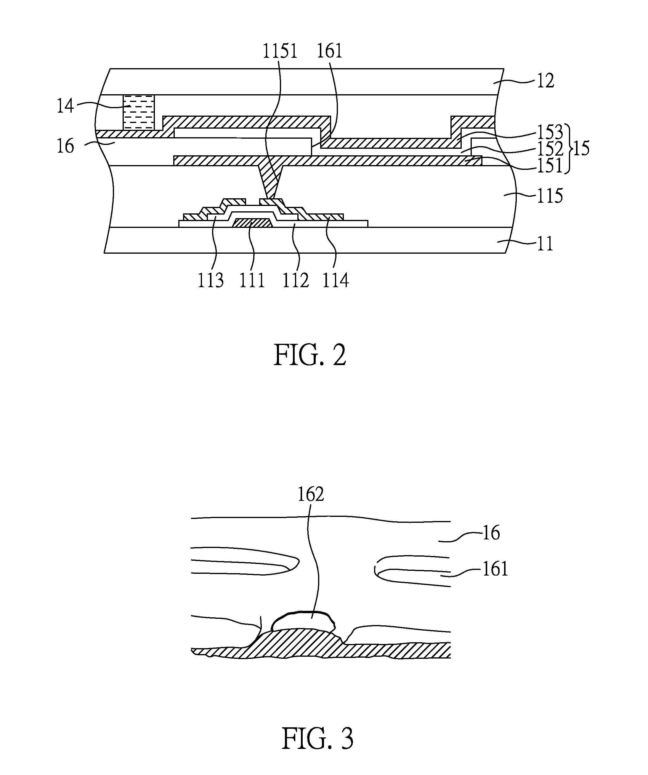
[0034]FIGS. 1A to 1B are cross-sectional views showing a process for assembling an OLED display panel of the present embodiment. As shown in FIG. 1, during the process for assembling an OLED display panel, a first substrate 11 and a second substrate 12 are firstly provided. Herein, organic light emitting (OLED) layers 15 and a pixel defining layer 16 are disposed on the first substrate 11, and the pixel defining layer 16 is disposed between two adjacent OLED layers 15. In the present embodiment, each OLED layer 15 can respectively emit red light, green light and blue light; but the color of light emitting from the OLED layers 15 is not limited thereto in other embodiment. In addition, plural spacers 14 are formed on the second substrate 12, and a frit sealant 13 is firstly formed on edges of the second substrate 12. Herein, the frit sealant 13 is formed thereon sequentially through a dispensing process and a sintering process.

[0035]Next, as shown in FIG. 1B, the first substrate 11 a...

embodiment 2

[0047]The structure of the OLED display panel of the present embodiment is similar to that of Embodiment 1, except for the following differences.

[0048]One difference is that the organic light emitting unit 15 used in the OLED display panel of the present embodiment comprises an organic light emitting layer 152 emitting white light, and a color filter 171 and a black matrix 172 are further disposed at the light-emitting side (i.e. between the second substrate 12 and the spacers 14), as shown in the cross-sectional view of FIG. 8 showing the OLED display panel of the present embodiment. Through the disposition of the color filter 171 and the black matrix 172, the OLED display panel of the present embodiment can emit light with different colors, such as red light, blue light and green light.

[0049]Another difference is that the light emitting region defined by the pixel opening 161 of the pixel defining layer 16 corresponds to the color filter 171, and the region outside the pixel openi...

embodiment 3

[0050]The structure of the OLED display panel of the present embodiment is similar to that of Embodiment 1, except for the following differences.

[0051]As shown in FIG. 10, the structure of the OLED display panel of the present embodiment is the same as that of Embodiment 1, except that the OLED display panel of the present embodiment is a bottom-emitting OLED display panel. Furthermore, in the OLED display panel of the present embodiment, only the first electrode unit 151 is a TCO electrode, and the second electrode 153 is a metal thin film electrode.


PUM


Abstract

An organic light emitting diode display panel is disclosed, which comprises: a first substrate with an organic light emitting layer formed thereon; a second substrate corresponding to the first substrate, and adhered to the first substrate with a frit sealant; and plural spacers disposed between the first substrate and the second substrate, and comprising a first spacer, a second spacer and a third spacer adjacent to each other, wherein shapes of a first projection of the first spacer, a second projection of the second spacer and a third projection of the third spacer on the second substrate are different from each other. In addition, the present invention also disclosed an organic light emitting diode display device containing the same.

Description

CROSS REFERENCE TO RELATED APPLICATION[0001]This application claims the benefits of the Taiwan Patent Application Serial Number 102134993, filed on Sep. 27, 2013, the subject matter of which is incorporated herein by reference.BACKGROUND OF THE INVENTION[0002]1. Field of the Invention[0003]The present invention relates to an organic light emitting diode (OLED) display panel and an OLED display device containing the same and, more particularly, to an OLED display panel with spacers having novel structures and an OLED display device containing the same.[0004]2. Description of Related Art[0005]Organic light-emitting diodes (OLEDs) are light in weight and ultra-thin in thickness, and also have advantages of high brightness, rapid response, wide viewing angles, no backlight requirement, low manufacturing cost and flexibility. Hence, OLEDs have great potential to apply on display panels of various electronic devices such as panels of cell phones, mobiles and MP3 players.[0006]During the p...

Claims


Application Information

Patent Timeline
IPC IPC(8): H01L27/32
CPCH01L27/3251H01L27/3246H10K59/17H10K50/8428H10K59/122H10K59/127
Inventor LIN, JENG-NANCHAO, KUANG-PINSUN, MING-CHIENCHU, HSIA-CHINGLIN, JIA-REN
Owner INNOLUX CORP
Why Eureka
Try Eureka