Reflective Optical Element

Active Publication Date: 2015-04-30
CARL ZEISS SMT GMBH
View PDF1 Cites 7 Cited by
  • Summary
  • Abstract
  • Description
  • Claims
  • Application Information

AI Technical Summary

Benefits of technology

[0009]It is an object of the present invention to provide a reflective optical element, in particular for a microlithographic projection exposure apparatus or for a mask inspection apparatus, which

Problems solved by technology

One problem that occurs in practice is that reflective optical elements designed for operation in the EUV, in particular owing to the absorption of the radiation emitted by the EUV light source, experience heating and an accompanying thermal expansion or deformation, which can in turn result in an impairment of the imaging properties of the optical system.
Transferring solution approaches known for VUV lithography systems (having an operating wavelength e.g. of appro

Method used


Image

  • Reflective Optical Element
  • Reflective Optical Element
  • Reflective Optical Element

Examples


Example

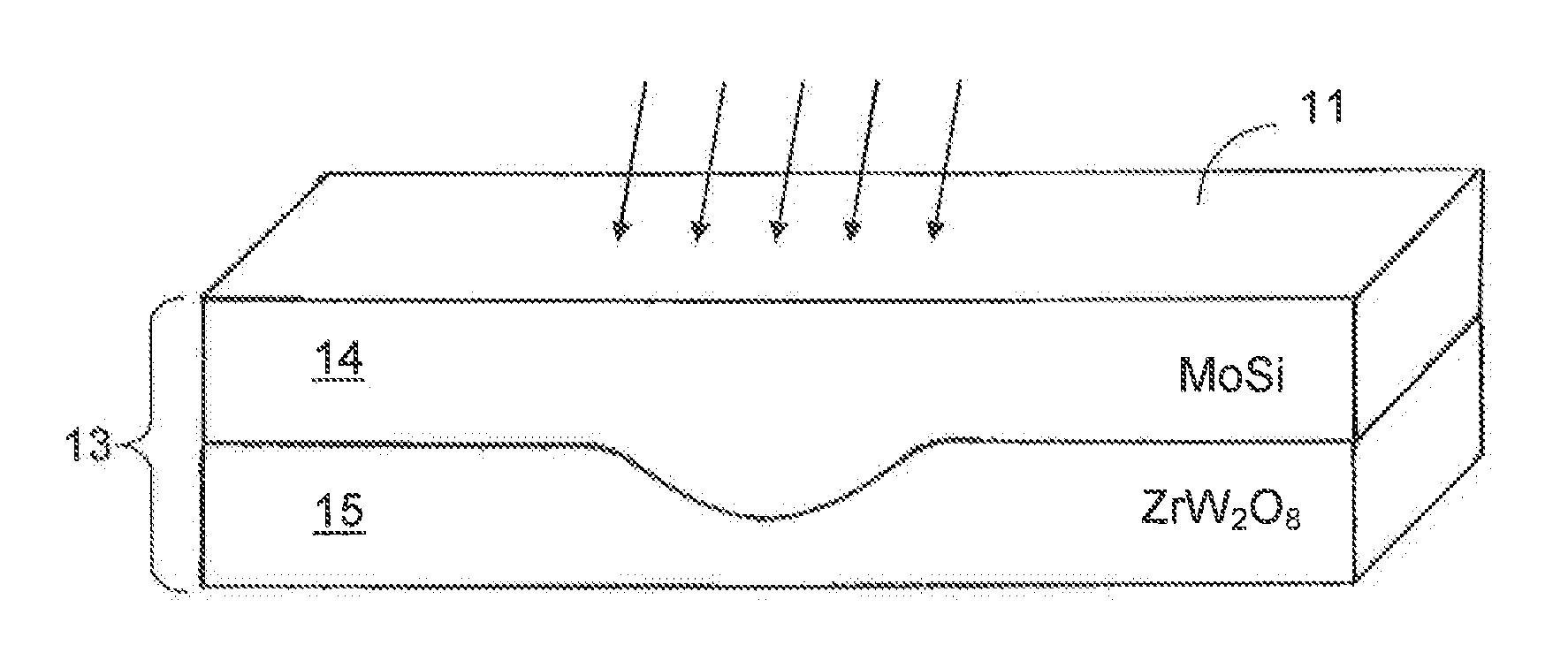
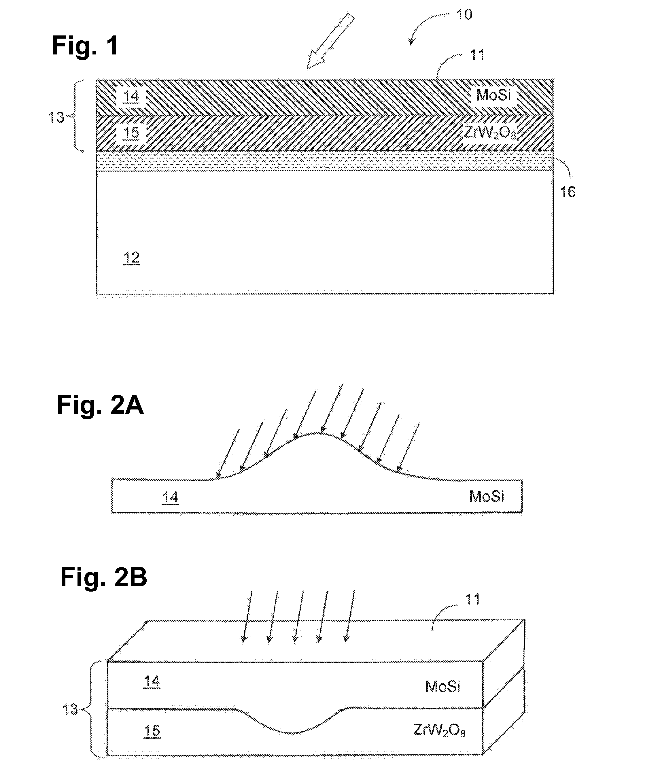
[0038]FIG. 1 shows a schematic illustration for explaining the construction of a reflective optical element according to the invention in a first embodiment of the invention. The reflective optical element 10 comprises in particular an element substrate 12 produced from an arbitrary suitable (mirror) substrate material. Suitable element substrate materials are e.g. titanium dioxide (TiO2)-doped quartz glass, wherein merely by way of an exemplary embodiment and without the invention being restricted thereto, the materials sold under the trademarks ULE® (from Corning Inc.) or Zerodur® (from Schott AG) can be used.

[0039]Furthermore, the reflective optical element 10 has a reflection layer system 14 in a manner known per se in principle, said reflective optical element, in the embodiment illustrated, comprising merely by way of example a molybdenum-silicon (Mo—Si) layer stack. Without the invention being restricted to specific configurations of said layer stack, a merely exemplary suita...


PUM


Abstract

A reflective optical element for a microlithographic projection exposure apparatus, a mask inspection apparatus or the like. The reflective optical element has an optically effective surface, an element substrate (12, 32, 42, 52), a reflection layer system (14, 34, 44, 54) and at least one deformation reduction layer (15, 35, 45, 55, 58). When the optically effective surface (11, 31, 41, 51) is irradiated with electromagnetic radiation, a maximum deformation level of the reflection layer system is reduced in comparison with a deformation level of an analogously constructed reflective optical element without the deformation reduction layer.

Description

CROSS-REFERENCE TO RELATED APPLICATIONS[0001]The following disclosure is based on and claims the benefit, under 35 U.S.C. §119(a), of German Patent Application No. 10 2013 222 140.1, filed on Oct. 30, 2013, which German Patent Application is incorporated in its entirety into the present application by reference.FIELD OF AND BACKGROUND OF THE INVENTION[0002]The invention relates to a reflective optical element, in particular for a microlithographic projection exposure apparatus or for a mask inspection apparatus.[0003]Microlithography is used for producing microstructured components, such as, for example, integrated circuits or LCDs. The microlithography process is carried out in a so-called projection exposure apparatus having an illumination device and a projection lens. The image of a mask (=reticle) illuminated with the illumination device is in this case projected by the projection lens onto a substrate (e.g. a silicon wafer) coated with a light-sensitive layer (photoresist) and...

Claims


Application Information

Patent Timeline
IPC IPC(8): G02B7/18G03F7/20G01N21/95
CPCG02B7/181G01N2201/0636G03F7/702G01N21/95G03F1/84G03F7/70316G03F7/70891G03F7/7095G21K1/062G21K2201/067G03F1/52
Inventor BITTNER, BORISWABRA, NORBERTSCHNEIDER, SONJASCHNEIDER, RICARDAWAGNER, HENDRIKILIEW, RUMENPAULS, WALTER
Owner CARL ZEISS SMT GMBH
Why Eureka
Try Eureka