Plasmonic nano-color coating layer and method for fabricating the same
- Summary
- Abstract
- Description
- Claims
- Application Information
AI Technical Summary
Benefits of technology
Problems solved by technology
Method used
Image
Examples
Embodiment Construction
[0034]Hereinafter, configuration and features of the present disclosure will be described based on embodiments, but these embodiments just exemplarily describe the present disclosure and are not intended to limit the present disclosure.
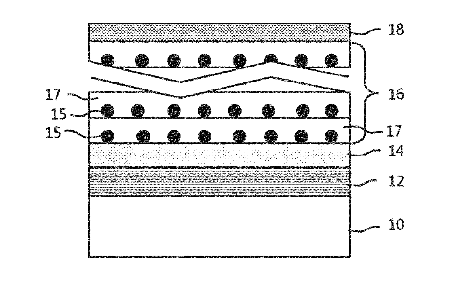
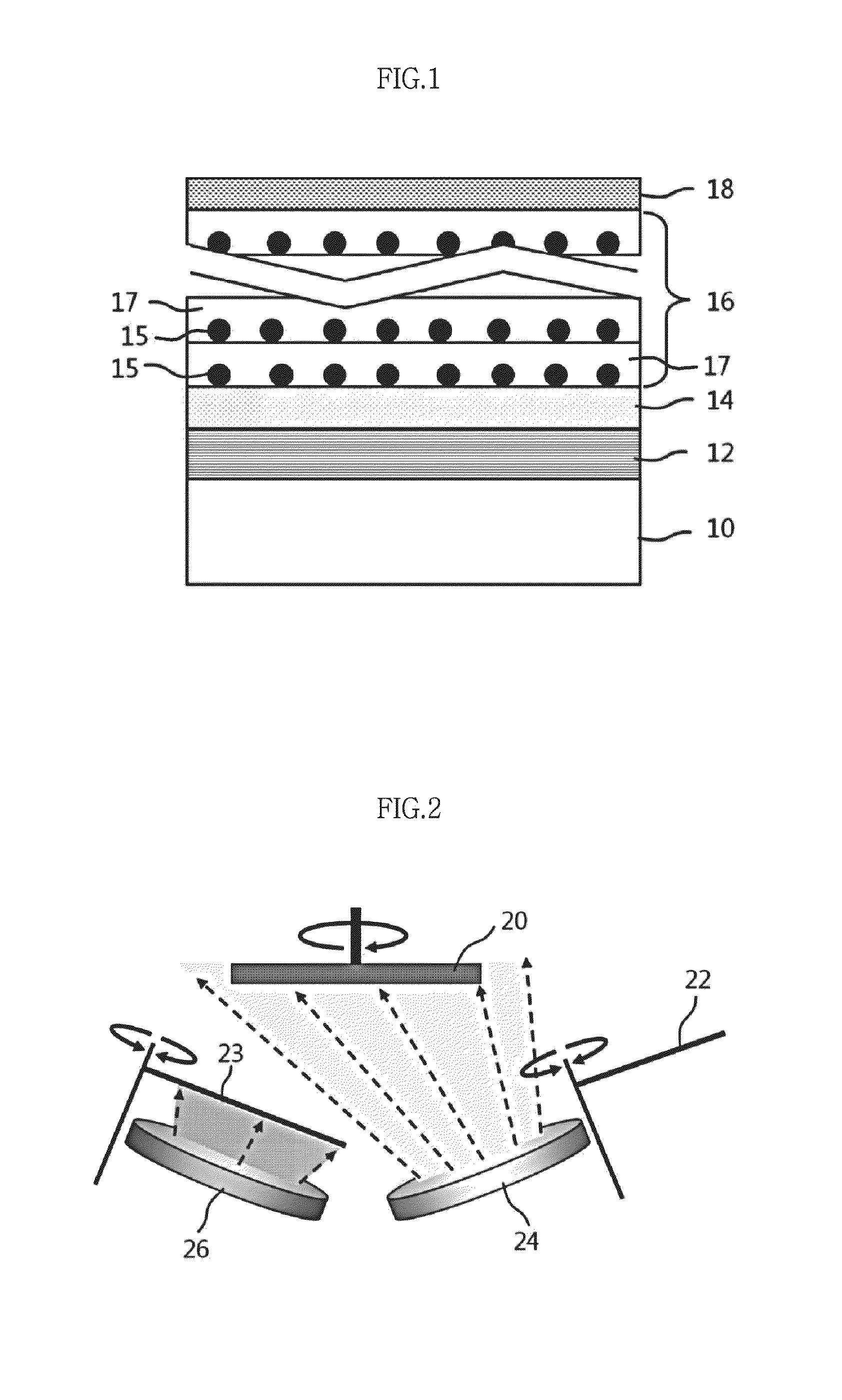
[0035]FIG. 1 is a cross-sectional view schematically showing a plasmonic nano-color coating layer according to an embodiment of the present disclosure, and the plasmonic nano-color coating layer may include a composite layer 16 having a plurality of metal nano-particle layers 15 and a plurality of matrix layers 17, a dielectric buffer layer 14 located below the composite layer 16 and a mirror layer 12 located below the dielectric buffer layer 14. The composite layer 16 may have a periodic multilayer structure in which the metal nano-particle layers 15 and the matrix layers 17 are alternately arranged. The plasmonic nano-color coating layer may be formed on a base body 10 to be colored.
[0036]If light is incident to the plasmonic nano-color coating laye...
PUM
| Property | Measurement | Unit |
|---|---|---|
| Thickness | aaaaa | aaaaa |
| Thickness | aaaaa | aaaaa |
| Thickness | aaaaa | aaaaa |
Abstract
Description
Claims
Application Information


