Imaging element, driving method, and electronic apparatus

a driving method and electronic equipment technology, applied in the direction of color television, television system scanning details, television systems, etc., can solve the problems of difficult to secure the voltage applied to the gate in the pixel, and achieve the effect of reducing voltage, high frame rate, and increasing sensitivity

Active Publication Date: 2015-05-07
SONY SEMICON SOLUTIONS CORP
View PDF5 Cites 26 Cited by
  • Summary
  • Abstract
  • Description
  • Claims
  • Application Information

AI Technical Summary

Benefits of technology

[0042]According to the first aspect of the present technology, a global shutter where a handling charge amount is large can be realized without providing a non-exposure period for an entire screen.
[0043]According to the second aspect of the present technology, a global shutter where a handling charge amount is large can be realized without providing a non-exposure period for an entire screen.
[0044]In addition, according to the second aspect of the present technology, a moving image having a high frame rate or an image in which a state of an instant of a subject moving fast is captured can be imaged and sensitivity increases at the same frame rate.
[0045]According to the third aspect of the present technology, a voltage can be decreased and a saturation signal amount can be increased.

Problems solved by technology

However, it is difficult to secure the voltage applied to the gate in the pixel, from the reason described above.

Method used


Image

  • Imaging element, driving method, and electronic apparatus
  • Imaging element, driving method, and electronic apparatus
  • Imaging element, driving method, and electronic apparatus

Examples


first embodiment

Configuration Example of Solid-State Imaging Element

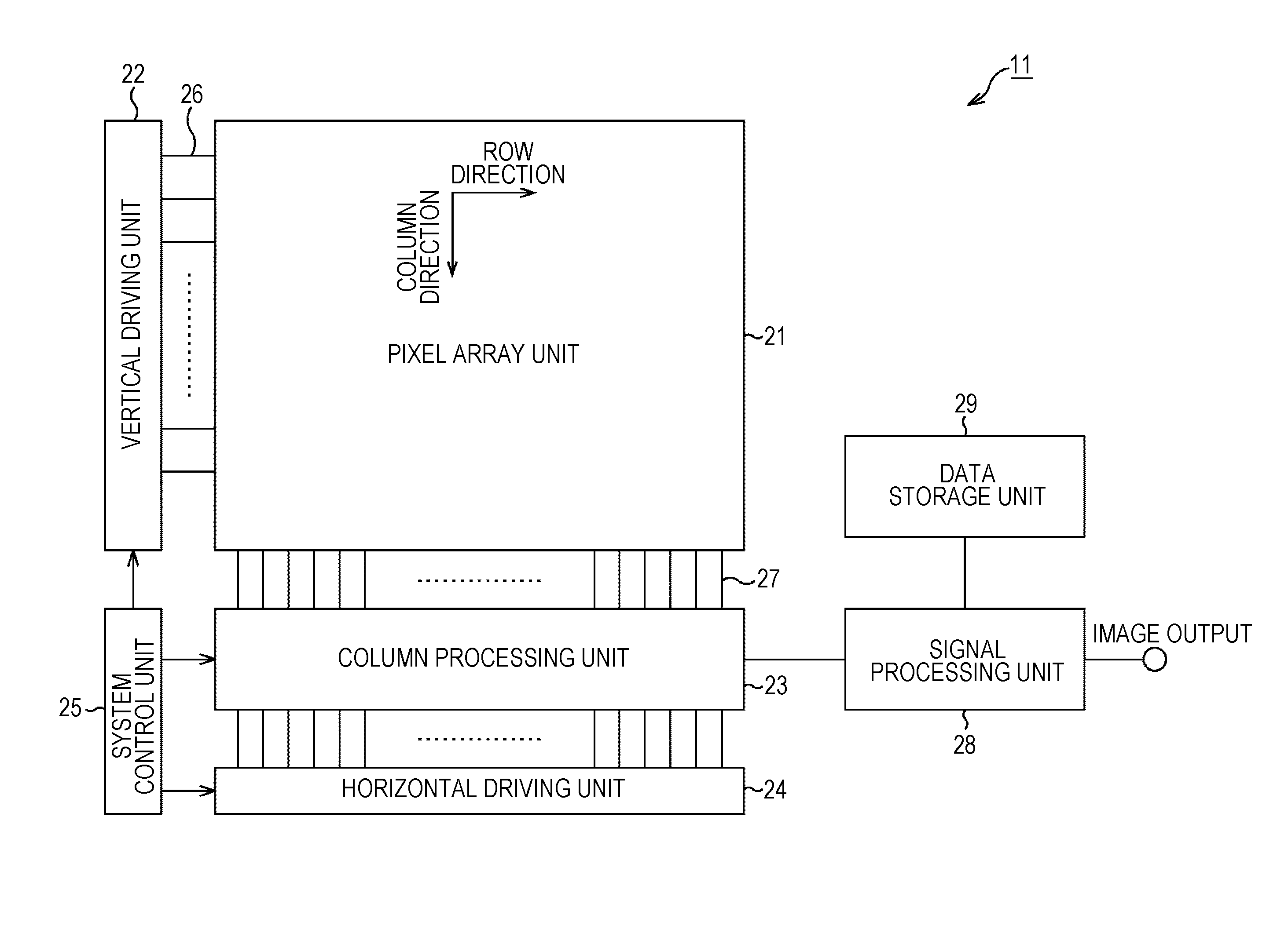
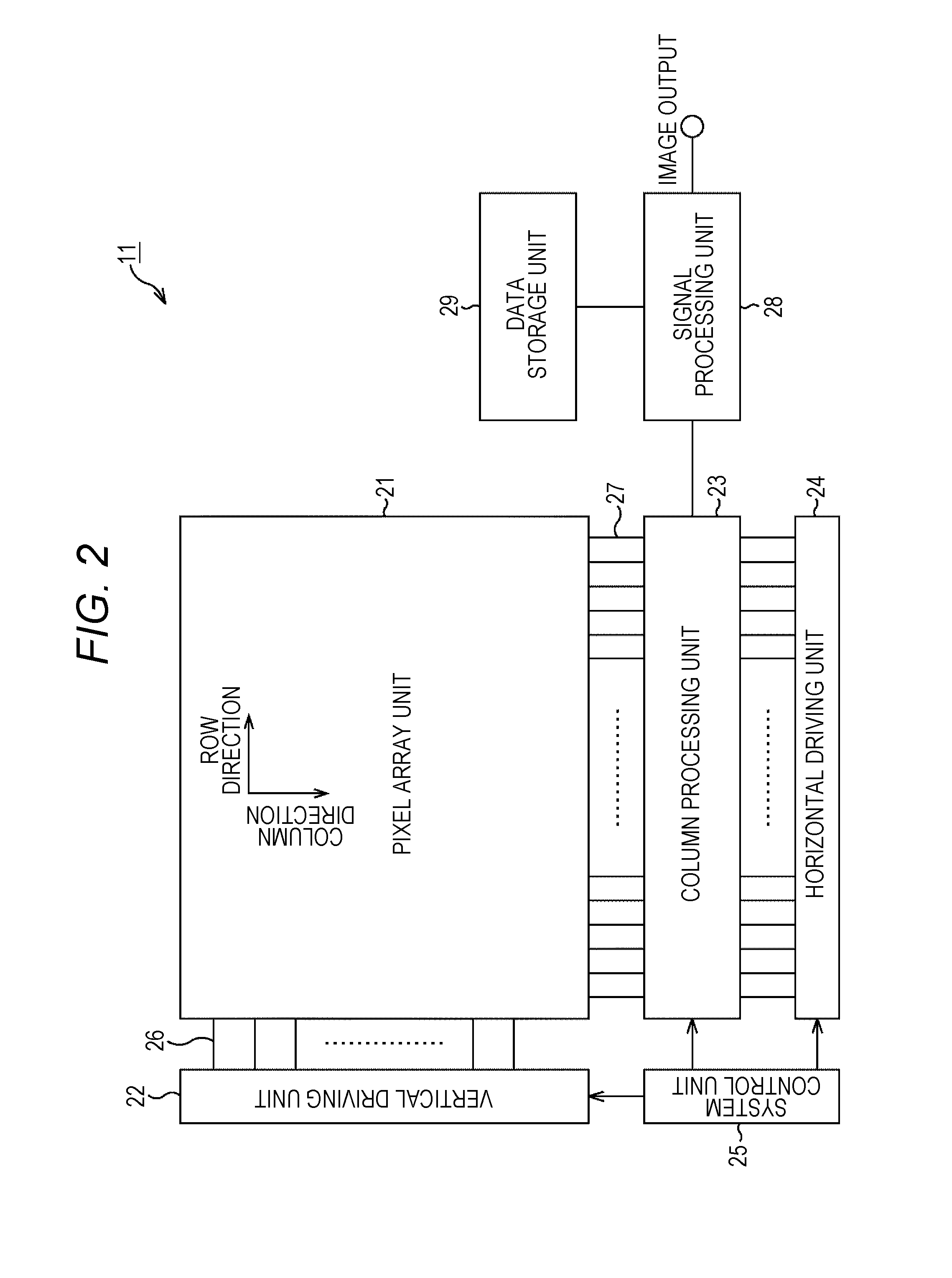
[0069]First, a configuration example of a solid-state imaging element to which the present technology is applied will be described. FIG. 2 is a diagram illustrating a configuration example of an embodiment of the solid-state imaging element to which the present technology is applied.

[0070]A solid-state imaging element 11 is configured from a CMOS image sensor, for example, and receives light from a subject, executes photoelectric conversion on the light, and generates an image signal, thereby imaging an image.

[0071]The solid-state imaging element 11 includes a pixel array unit 21, a vertical driving unit 22, a column processing unit 23, a horizontal driving unit 24, a system control unit 25, pixel driving lines 26, vertical signal lines 27, a signal processing unit 28, and a data storage unit 29.

[0072]In the solid-state imaging element 11, the pixel array unit 21 is formed on a semiconductor substrate (chip) not illustrated in the ...

second embodiment

With Respect to Structure of Each Pixel

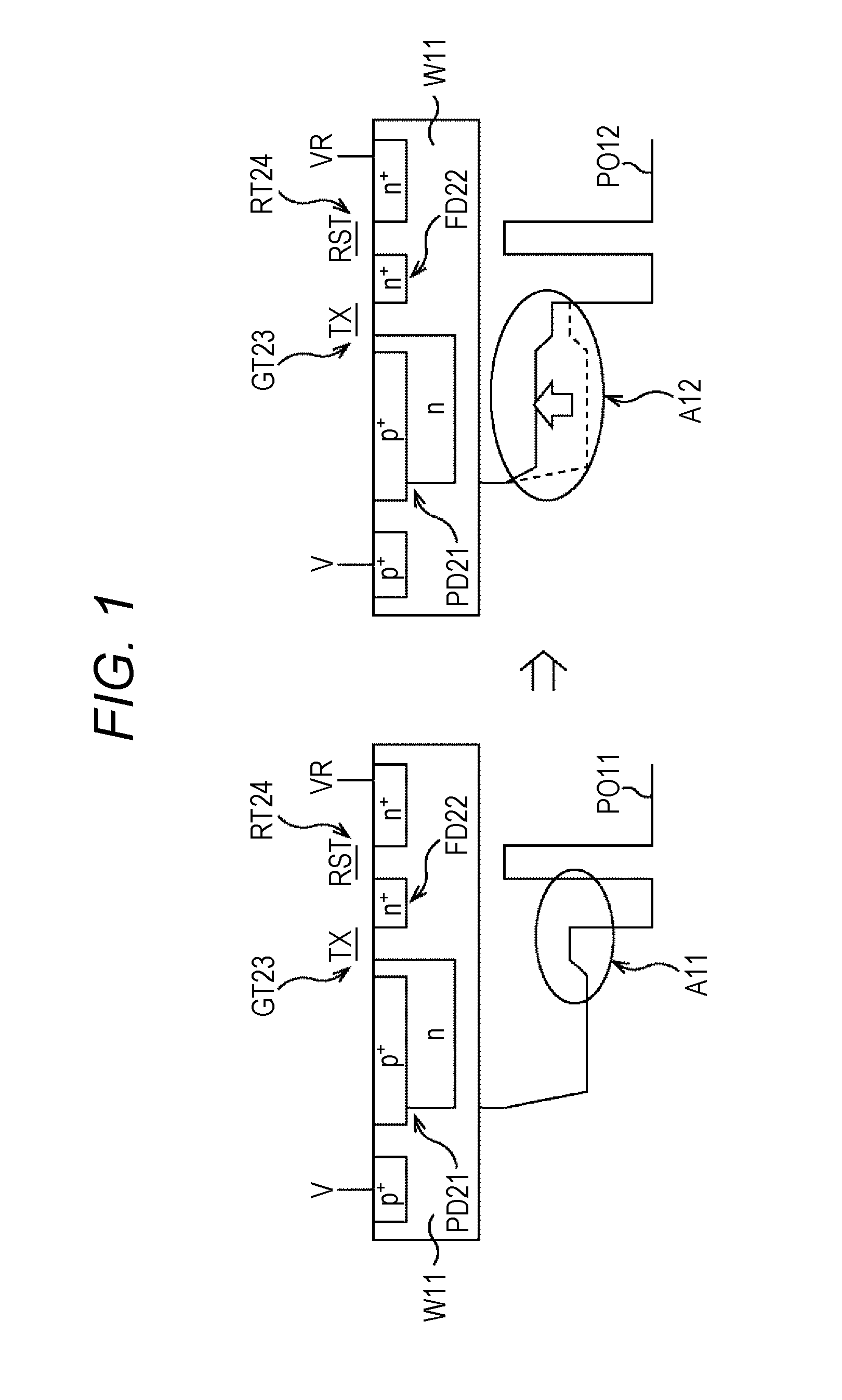
[0127]A structure of the pixel illustrated in FIG. 3 will be described. FIG. 10 is a diagram illustrating the structure of the pixel illustrated in FIG. 3. In FIG. 10, a plane pattern illustrating a pixel layout and cross-sections taken along A-A′ and B-B′ in the plane pattern, respectively, are illustrated. In FIG. 10, portions corresponding to those in the case of FIG. 3 are denoted with the same reference numerals and explanation thereof is appropriately omitted.

[0128]As illustrated in the cross-section taken along B-B′, a photodiode 61 has a configuration of a diode of a PN junction obtained by forming an N-type semiconductor region 101 in a P-type well 52 on a semiconductor substrate 51. The photodiode 61 becomes an embedded photodiode in which a P-type semiconductor region 102 is formed in a surface layer portion thereof and a depletion end is separated from an interface.

[0129]A first transfer gate unit 63 has a configuration in which a g...

third embodiment

Modification of Third Embodiment

With Respect to Operation of Solid-State Imaging Element

[0245]In addition, for example, as illustrated in FIG. 18, a negative voltage may be applied to the P-type well 52 when the charges are transferred from the photodiode 61 to the charge / voltage converting unit 68 and assistance of the charge transfer may be performed.

[0246]FIG. 18 illustrates a state of each signal supplied to a pixel at each time. That is, in the drawing, a horizontal direction shows a time and a longitudinal direction shows a level (voltage) of each signal. In addition, polygonal lines SL41 to SL45 show driving signals SEL, TG, RST, a pulse Pwell, and a driving signal GC, respectively.

[0247]In an example of FIG. 18, an operation until just before a time t43 after the imaging operation of the image starts is the same as the operation until just before the time t33 in FIG. 17. That is, at the time t41, the driving signals SEL, RST, and GC are turned on and the pulse Pwell is turne...


PUM

PropertyMeasurementUnit
timeaaaaaaaaaa
imaging functionaaaaaaaaaa
voltageaaaaaaaaaa

Abstract

The present technology relates to an imaging element, a driving method, and an electronic apparatus that can decrease a voltage and increase a saturation signal amount.
In each pixel configuring a pixel array unit, a photodiode receiving light from a subject and performing photoelectric conversion on the light and a first charge accumulating unit accumulating charges generated by the photodiode are provided. A reset gate unit to initialize the first charge accumulating unit is connected to the first charge accumulating unit through a third transfer gate unit. When the first charge accumulating unit is initialized, a voltage is applied to gate electrodes of the third transfer gate unit and the reset gate unit and a positive voltage is applied to a well region provided with a pixel to assist voltage application. Thereby, initialization is appropriately performed and a reset level is suppressed low. As a result, a voltage can be decreased and a saturation signal amount can be increased. The present technology can be applied to a solid-state imaging element.

Description

TECHNICAL FIELD[0001]The present technology relates to an imaging element, a driving method, and an electronic apparatus and particularly, to an imaging element, a driving method, and an electronic apparatus that enable a global shutter to be realized.BACKGROUND ART[0002]As imaging elements mounted to a digital video camera, complementary metal oxide semiconductor (CMOS) image sensors (hereinafter, simply referred to as the CISs) have been known. Among the CISs, there is a CIS that has a function called a global shutter in which simultaneity of an exposure time of an image to be imaged has been secured.[0003]In addition, with the miniaturization of a semiconductor process, a voltage applied to a gate of an element such as a metal oxide semiconductor field effect transistor (MOSFET) has decreased.[0004]For example, a relatively high voltage is applied to a gate provided in a pixel of the CMOS image sensor and initialization of each element in the pixel or signal transmission from a p...

Claims


Application Information

Patent Timeline
Patent Type & Authority Applications(United States)
IPC IPC(8): H04N5/353H04N5/378H04N5/374
CPCH04N5/353H04N5/378H04N5/374H01L27/14609H01L27/14603H04N25/531H04N25/589H04N25/59H04N25/74H04N25/771H04N25/53H04N25/75H04N25/76
Inventor MABUCHI, KEIJISAKAKIBARA, MASAKI
Owner SONY SEMICON SOLUTIONS CORP
Why Eureka
Try Eureka