

Light exposure system and light exposure process
a light exposure system and light exposure technology, applied in photomechanical treatment, printing, instruments, etc., can solve the problems of failure of reliability test, damage to the inside components of the panel or the polymer thin film on the glass substrate, and poor optical performance of the lcd panel. , to achieve the effect of enhancing the optical performance or reliability of the product and reducing the damage to the inside components
- Summary
- Abstract
- Description
- Claims
- Application Information
AI Technical Summary
Benefits of technology
Problems solved by technology
Method used
Image

Examples
Embodiment Construction
[0031]The present invention will be apparent from the following detailed description, which proceeds with reference to the accompanying drawings, wherein the same references relate to the same elements.
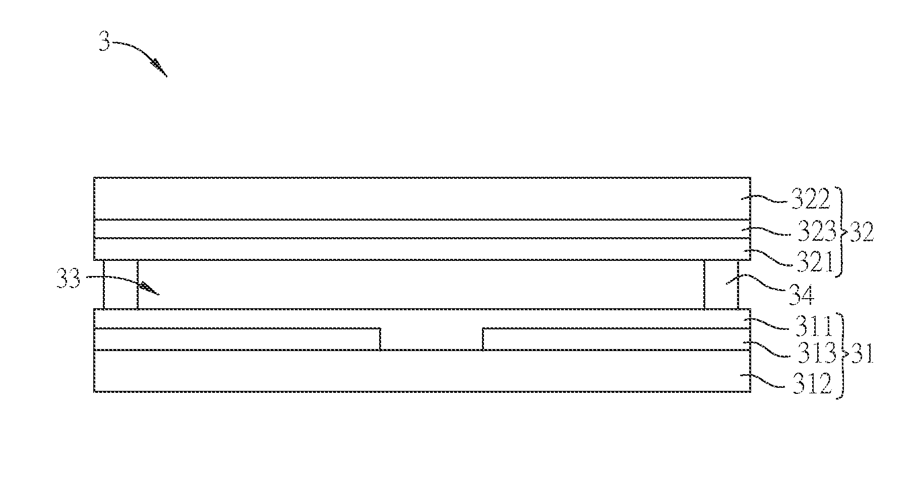
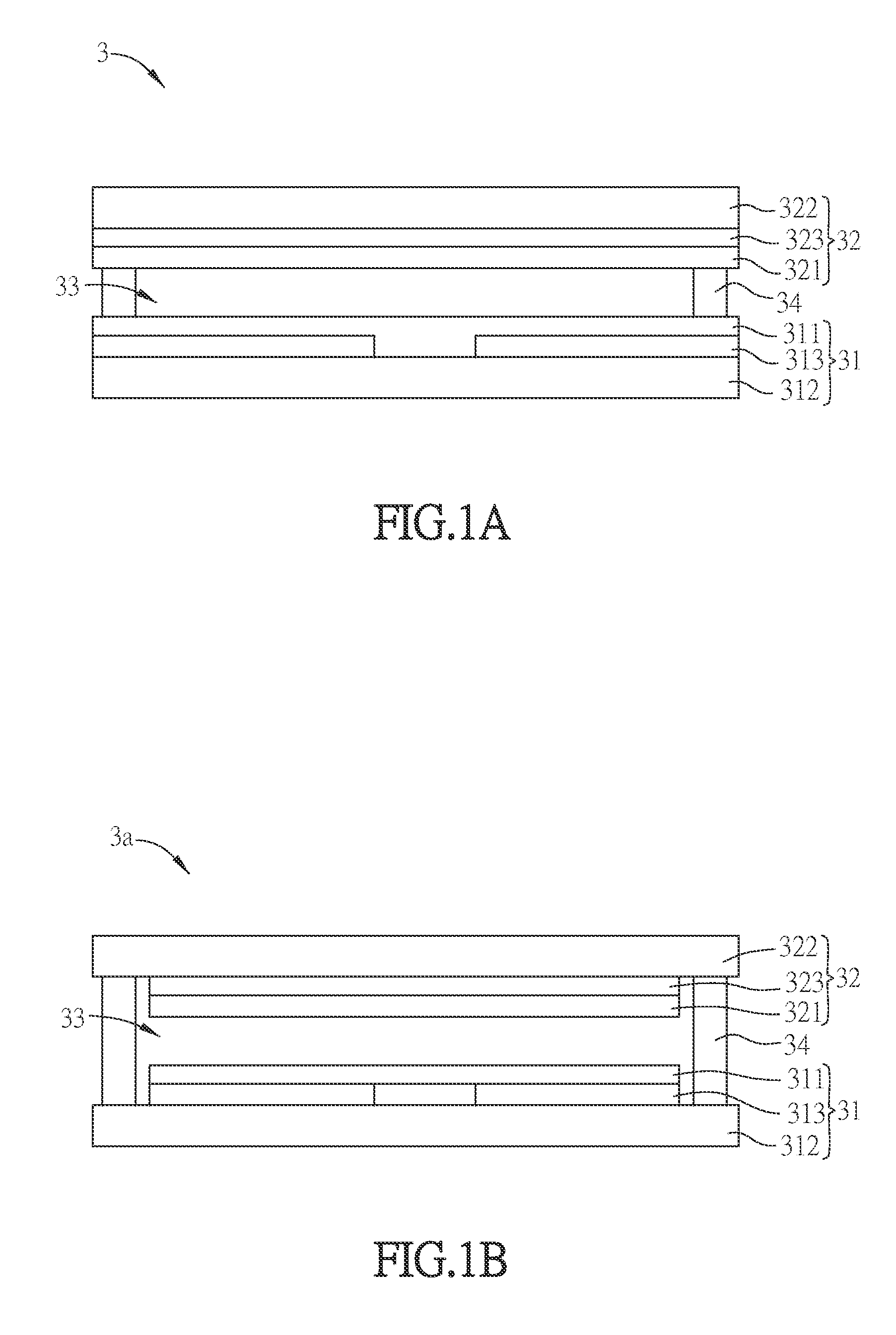
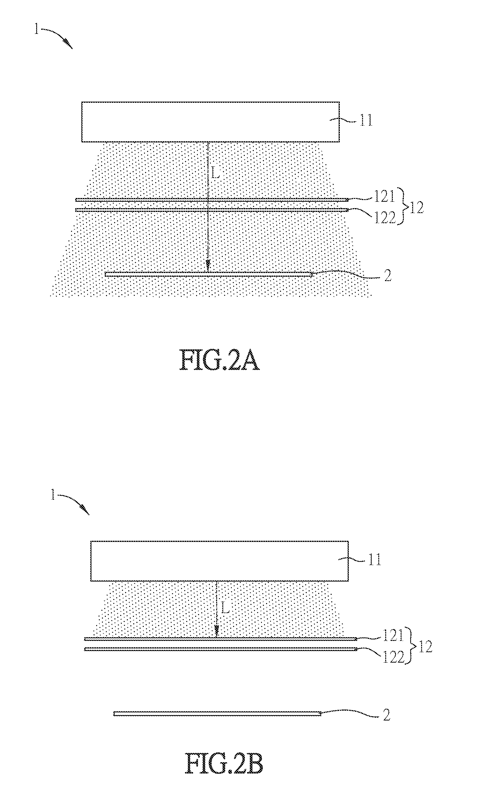
[0032]The light exposure system can execute a light exposure process to an assembly liquid crystal cell, so that the photosensitive monomers within the liquid crystal of the assembly liquid crystal cell are polymerized to become a polymer alignment layer that is capable of controlling the arrangement of the liquid crystal. Herein, the so-called assembly liquid crystal cell indicates that the assembly of the upper and lower substrates and the filling of the liquid crystal has been completed but the scribing has not been performed so that the product of a display panel is not generated yet. An assembly liquid crystal cell can include a display panel (including an upper substrate, a lower substrate and a liquid crystal layer) or include a plurality of display panels (including a mother g...
PUM
| Property | Measurement | Unit |
|---|---|---|
| angle | aaaaa | aaaaa |
| photosensitive | aaaaa | aaaaa |
| time | aaaaa | aaaaa |
Abstract
Description
Claims
Application Information