Method of forming metal lines having high conductivity using metal nanoparticle ink on flexible substrate

a metal nanoparticle and flexible substrate technology, applied in the direction of cable/conductor manufacturing, conductive pattern formation, microstructural device assembly, etc., can solve the problems of low process reproducibility, poor conductivity characteristics, short process time, etc., to facilitate stamping and high heat resistance. , the effect of high conductivity

Inactive Publication Date: 2015-06-18
KYUNGPOOK NAT UNIV IND ACADEMIC COOP FOUND
View PDF3 Cites 10 Cited by
  • Summary
  • Abstract
  • Description
  • Claims
  • Application Information

AI Technical Summary

Benefits of technology

[0024]According to a method of forming metal lines according to the present invention, after metal lines using a metal nanoparticle ink is formed on a substrate having high heat resistance, a thermal treatment/sintering process is performed at a high temperature, and the metal lines are transfer-printed on a flexible substrate, so that it is possible to perform the thermal treatment/sintering process on the metal nanoparticle ink at a high temperature. As a result, it is possible to form the metal lines having high conductivity on the flexible substrate.
[0025]In addition, according to a method of forming metal lines according to the present invention, a buffer layer is formed, and supporting members are formed between a substrate and metal lines by etching the buffer layer so as for a portion of the buffer layer to remain, so that the picking-up by the stamp is facilitate, and a transfer printing process can be applied in the state where a shape of a pattern can be maintained.
[0

Problems solved by technology

However, in the case of forming the metal lines by using the metal nanoparticle ink, since the metal lines can be formed through a direct printing process, the process time is shortened, and a vacuum state is unnecessary in the process.
Because of the aggregation, in the case of forming the metal line electrodes through the printing process, there is a problem in that a uniformity characteristic and a conductivity characteristic become bad and process reproducibility becomes low.
However, since most of the materials of enhancing the degree of dispersion or the surfactants have an insulating property, in the state where the metal line electrode is formed by using these materials, the conductivity characteristic becomes very bad because of the insulating property of the aforementioned materials arranged between the metal nanoparticles.
In addition, since a cross-linking material mixed in order to derive the thin film formed through a printing process so as to have a stable adhesion characteristic on the substrate and in order to prevent crack and deformation of the thin film is also a material having an insulating property, there is a problem in that the metal line electrode has a bad conductivity characteristic because of the material having an insulating prope

Method used


Image

  • Method of forming metal lines having high conductivity using metal nanoparticle ink on flexible substrate
  • Method of forming metal lines having high conductivity using metal nanoparticle ink on flexible substrate
  • Method of forming metal lines having high conductivity using metal nanoparticle ink on flexible substrate

Examples


first embodiment

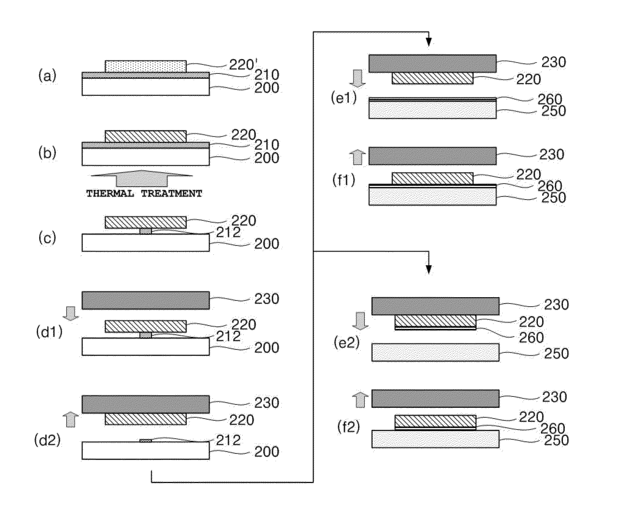
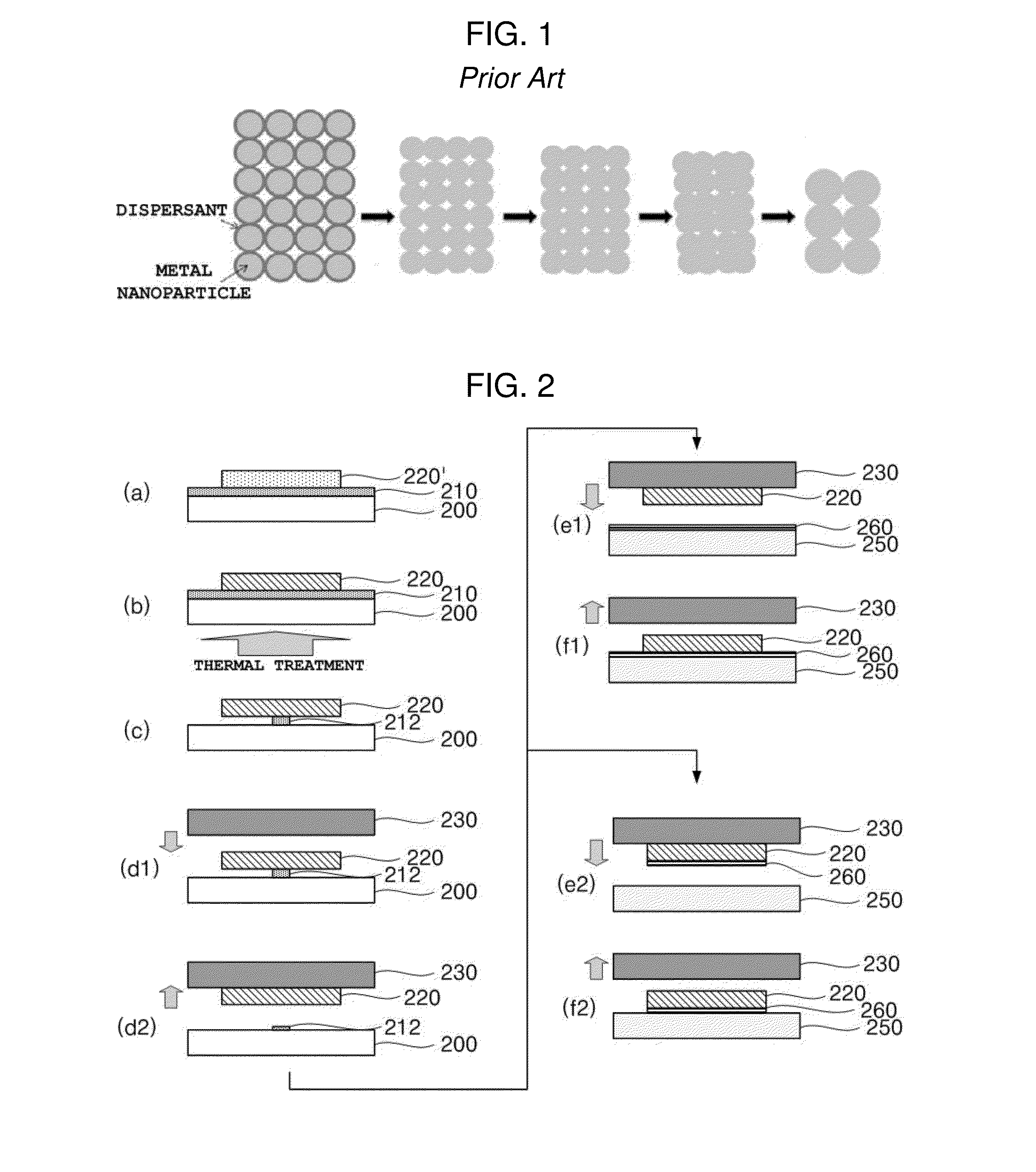
[0042]Hereinafter, a metal line forming method according to an exemplary first embodiment of the present invention will be described in detail with reference to the attached drawings. FIG. 2 is a diagram illustrating a sequence of processes of the metal line forming method according to the first embodiment.

[0043]Referring to (a) of FIG. 2, in the metal line forming method according to the first embodiment of the present invention, first, a buffer layer 210 is formed on a first substrate 200, and after that, metal lines are formed by printing a metal nanoparticle ink 220 over the buffer layer.

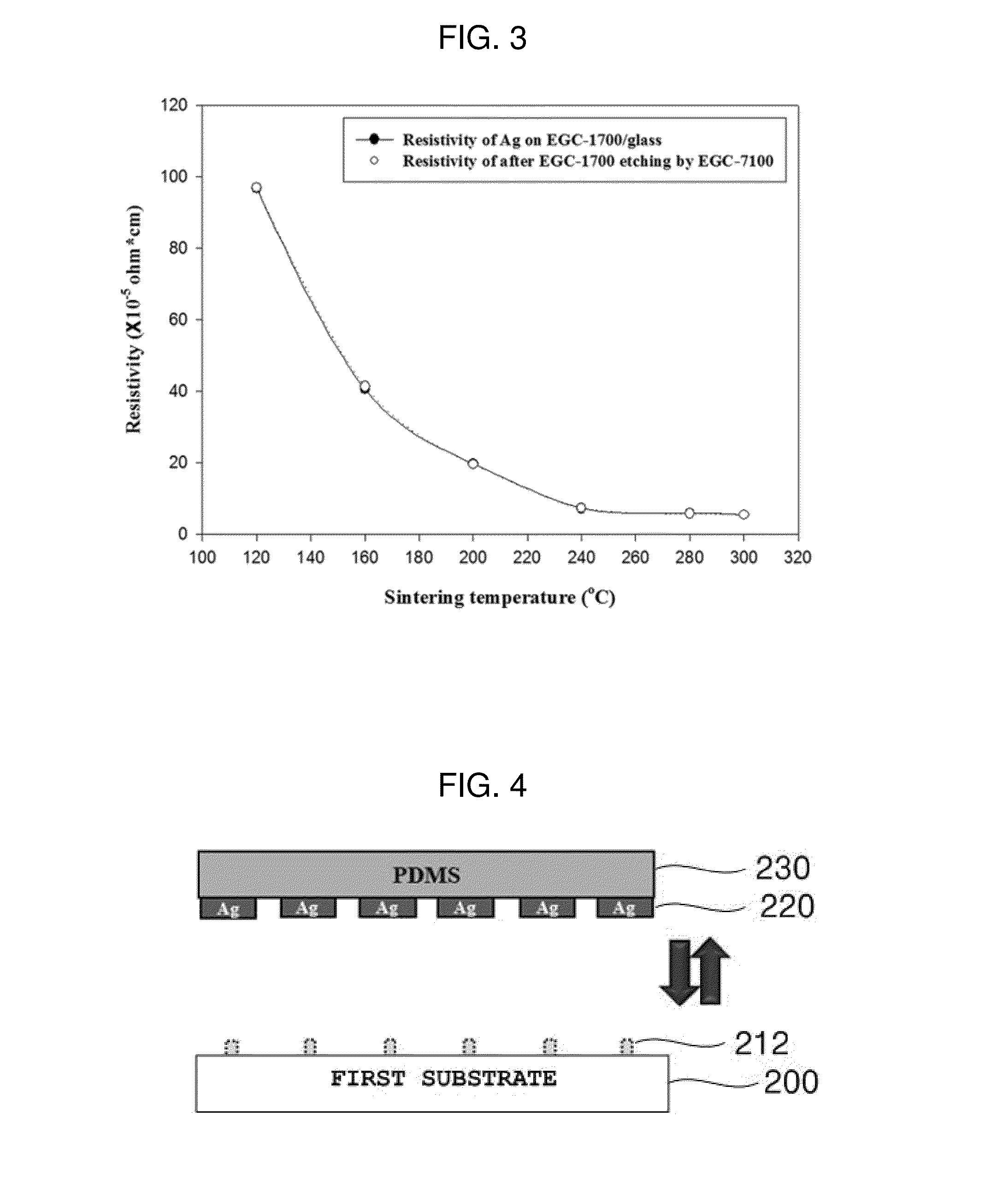
[0044]The buffer layer 210 may be formed by using a solution having low viscosity and low surface tension and containing fluorochemical acrylic polymers in a hydrofluoroether solvent or a material which is processable in a printing process and an additional etching process. The buffer layer may be formed by using, for example, NOVEC™ 1700 Electronic Grade Coating” (trade name, produced by 3M™).

[...

second embodiment

[0063]Hereinafter, a metal line forming method according to a second embodiment of the present invention will be described in detail with reference the attached drawings. FIG. 8 is is a diagram illustrating a sequence of processes of the metal line forming method according to the second embodiment of the present invention.

[0064]Referring to (a) of FIG. 8, in the metal line forming method according to the second embodiment of the present invention, first, a buffer layer 810 is formed on a first substrate 800 through a printing process, and after that, metal lines are formed by printing a metal nanoparticle ink 820′ over the buffer layer. In the embodiment, the metal nanoparticle ink, the first substrate, and a second substrate are the same as those of the first embodiment. In addition, in the embodiment, a printing process for the metal nanoparticle ink is the same as that of the first embodiment.

[0065]The buffer layer 810 may be formed by using a solution having a low viscosity and ...

third embodiment

[0072]Hereinafter, a highly-conductive metal line forming method on a flexible substrate by using a metal nanoparticle ink according to a third embodiment of the present invention will be described in detail. The metal line forming method according to the third embodiment is different from the first and second embodiments where a flat stamp is used. In the third embodiment, a transfer process is performed by using a stamp having a patterned mold, so that metal lines can be selectively picked up from a first substrate according to a shape of the stamp having the patterned mold in transfer printing.

[0073]The stamp used in the metal line forming method according to the third embodiment is different from the stamps in the metal line forming method according to the first and second embodiments in terms of a shape. FIG. 5 is conceptual cross-sectional diagram illustrating a pick-up process using the stamp 330 having the patterned mold in the metal line forming method according to the thir...


PUM


Abstract

Provided is a method of forming metal-lines having high conductivity on a flexible substrate, including (a) forming a buffer layer on a first substrate, (b) forming metal-lines by printing a metal-nanoparticle-ink on the buffer layer, (c) sintering the metal-nanoparticle-ink through thermal treatment, (d) forming supporting-members between the metal-lines and the first substrate by etching the buffer layer by using a etching solvent and controlling an etching time so that a portion of the buffer layer is not etched, (e) picking up the metal-lines from the first substrate by using a stamp in the state where a pattern of the metal-lines is fixed and arranged by the supporting-members, and (f) transferring the picked-up metal-lines to a second substrate, wherein the first substrate is a heat resistant substrate which is not deformed at a sintering temperature of the metal-nanoparticle-ink, and the second substrate is a flexible substrate.

Description

[0001]This application claims priority to Korean Patent Application No. 10-2013-0156505, filed on Dec. 16, 2013, and all the benefits accruing therefrom under 35 U.S.C. §119, the contents of which in its entirety are hereby incorporated by reference.BACKGROUND OF THE INVENTION[0002]1. Field of the Invention[0003]The present invention relates to a method of forming metal lines on a flexible substrate, and more particularly, to a method of forming metal lines having high conductivity on a flexible substrate by forming the metal lines by printing a metal nanoparticle ink on a heat resistant substrate, by performing a thermal treatment / sintering process at a high temperature to allow the metal lines to have a high conductivity characteristic, and after that, by transfer-printing the metal lines on the flexible substrate.[0004]2. Description of the Prior Art[0005]Recently, with increasing expectations and demands for flexible electronic devices, much attention has been drawn by a techniq...

Claims


Application Information

Patent Timeline
IPC IPC(8): H05K3/00H05K3/12
CPCH05K3/007H05K2203/1131H05K2203/06H05K3/1291H05K1/0393H05K1/097H05K3/207H05K3/386B81C3/00H01B13/00H05K3/12H05K3/20
Inventor KIM, HAK-RINBAE, JIN-HYUKPARK, JI-SUB
Owner KYUNGPOOK NAT UNIV IND ACADEMIC COOP FOUND
Why Eureka
Try Eureka