

HYBRID NAND WITH ALL-BL m-PAGE OPERATION SCHEME
a hybrid array and operation scheme technology, applied in static storage, digital storage, instruments, etc., can solve the problems of serious degradation of nand data quality and reliability, severe coupling effects of inter-wl and inter-bl cells, and more latency and power consumption in all operations and usages. achieve the effect of saving circuit size, flexible and effectiv
- Summary
- Abstract
- Description
- Claims
- Application Information
AI Technical Summary
Benefits of technology
Problems solved by technology
Method used
Image

Examples
Embodiment Construction
[0153]In the following detailed description of the present embodiments, reference is made to the accompanying drawings that forms a part hereof, and in which is shown, by way of illustration, specific embodiments in which the disclosure may be practiced. In the drawings, like numerals describe substantially similar components throughout the several views. These embodiments are described in sufficient detail to enable those skilled in the art to practice the embodiments. Other embodiments may be utilized and structural, logical, and electrical changes may be made without departing from the scope of the present disclosure. The following detailed description, therefore, not to be taken in a limitation sense.
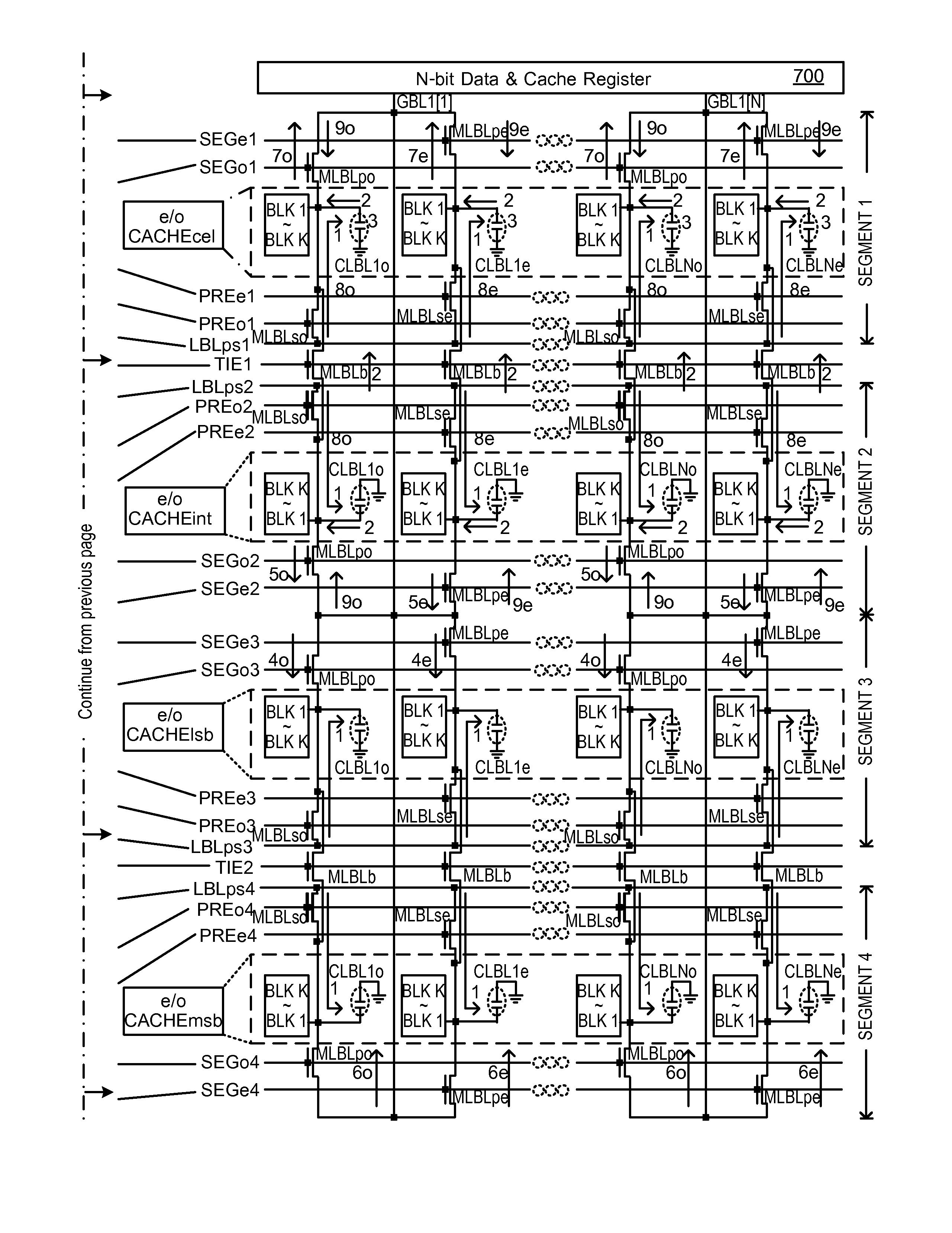
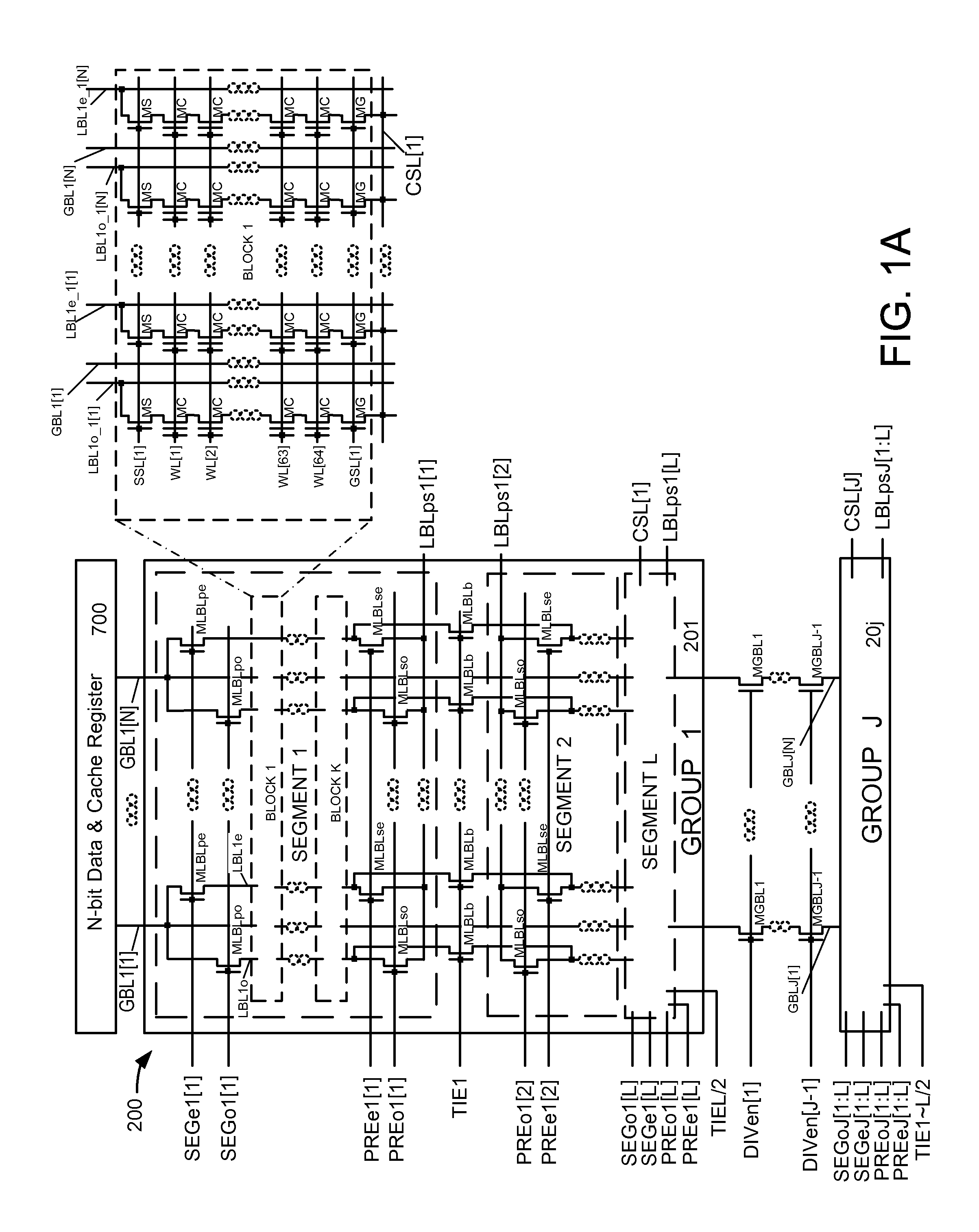
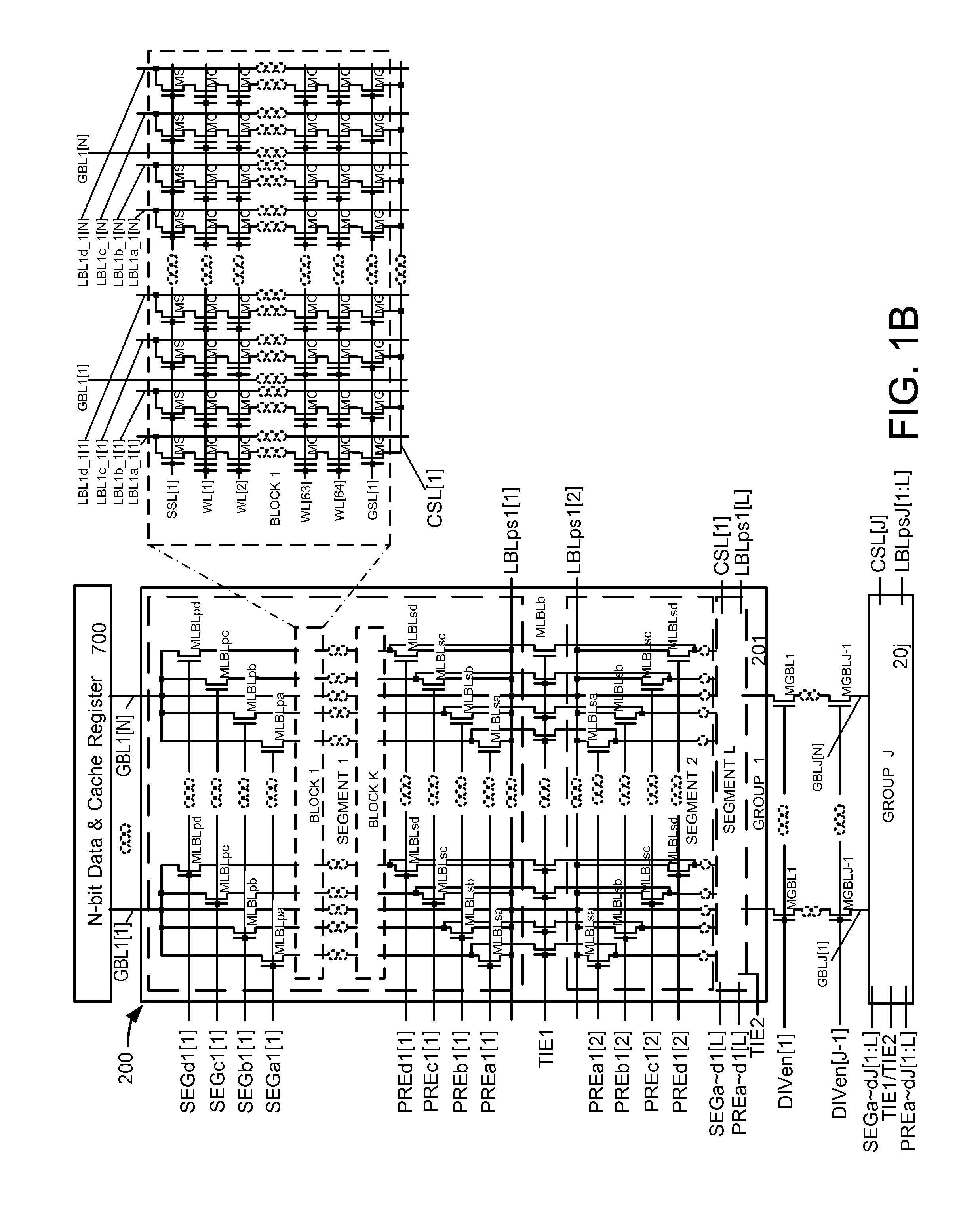
[0154]FIG. 1A shows an embodiment of a preferred 2D HiNAND2 array 200 with 2-level, 2-metal top global metal2 GBL and bottom local metal1 LBL hierarchical Even and Odd numbered cell array that comprises J divided Groups with option of equal or unequal sizes. In this example, whole H...
PUM
 Abstract
Description
Claims
Application Information