A semiconductor device comprising a surface portion implanted with nitrogen and fluorine

a surface portion and semiconductor technology, applied in semiconductor devices, semiconductor/solid-state device details, electrical devices, etc., can solve the problems of poor adhesion between films, bridge defects, cracks, peeling or leakage current of devices, etc., to achieve low surface roughness, high adhesion, and low surface d

Active Publication Date: 2015-07-02
MACRONIX INT CO LTD
View PDF6 Cites 0 Cited by
  • Summary
  • Abstract
  • Description
  • Claims
  • Application Information

AI Technical Summary

Benefits of technology

[0005]The present invention provides a semiconductor device and a method of fabricating the same, in which a dielectric layer is formed with low surface defect, low surface roughness and high adhesion to another material layer.
[0027]In view of the above, with the fabricating method of the semiconductor device of the invention, the surface defects of the dielectric layer can be effectively removed, the surface roughness of the dielectric layer can be significantly decreased, and the adhesion within the film stack can be greatly improved. In other words, the dielectric layer of the semiconductor device of the invention can be formed with low surface defect, low roughness and high adhesion to another material layer, so that the performance of the device can be greatly improved.

Problems solved by technology

In the following patterning processes such as photolithography and etching processes, the high roughness of the dielectric layer causes poor adhesion between films in the film stack, or even results in bridge defects, cracks, peeling or leakage current of the device.

Method used


Image

  • A semiconductor device comprising a surface portion implanted with nitrogen and fluorine
  • A semiconductor device comprising a surface portion implanted with nitrogen and fluorine
  • A semiconductor device comprising a surface portion implanted with nitrogen and fluorine

Examples


Embodiment Construction

[0035]Reference will now be made in detail to the present preferred embodiments of the invention, examples of which are illustrated in the accompanying drawings. Wherever possible, the same reference numbers are used in the drawings and the description to refer to the same or like parts.

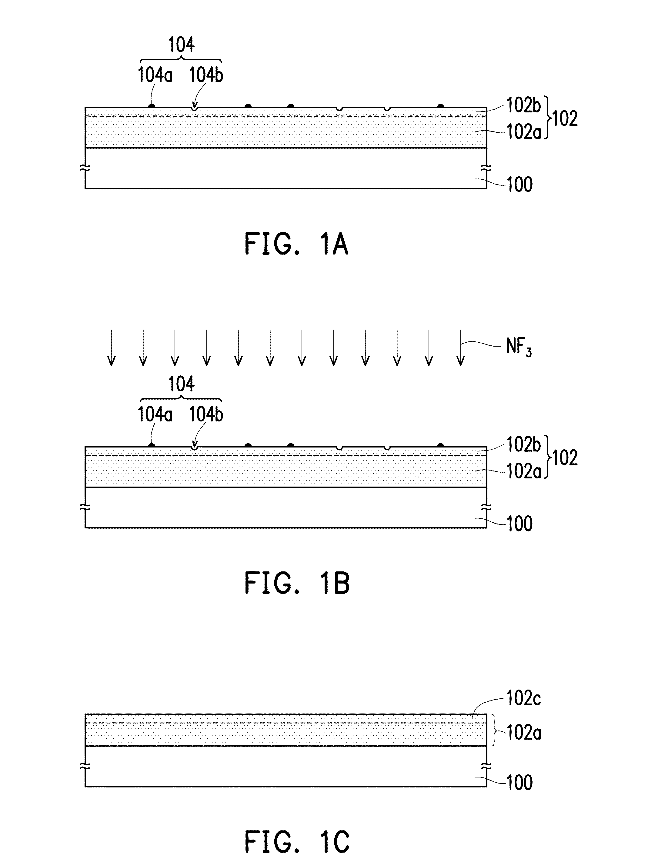
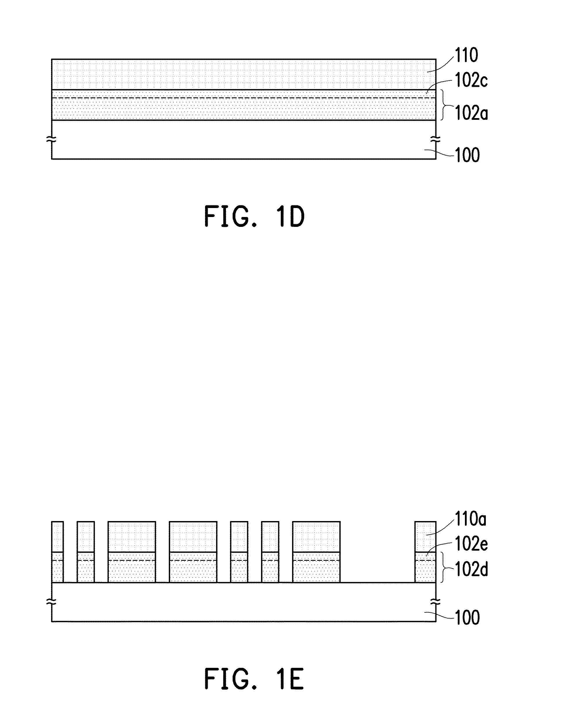
[0036]FIG. 1A to FIG. 1E are schematic cross-sectional views of a method of fabricating a semiconductor device according to an embodiment of the present invention.

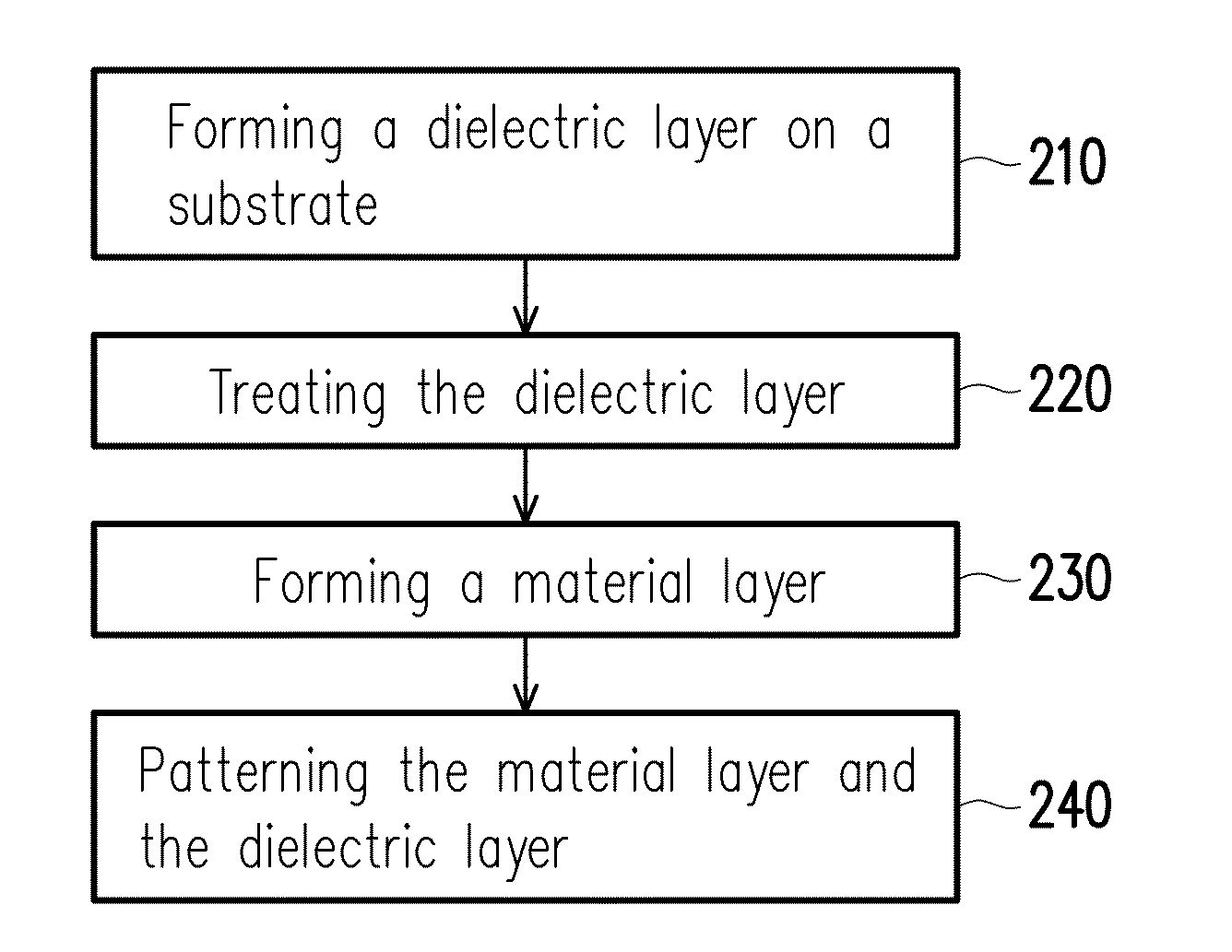
[0037]FIG. 2 is a flow chart of a method of fabricating a semiconductor device according to an embodiment of the present invention.

[0038]Referring to FIG. 1A and FIG. 2, a step 210 in implemented, in which a dielectric layer 102 is formed on a substrate 100. The substrate 100 can be a semiconductor substrate, such as a silicon substrate. The substrate 100 can be a silicon-on-insulator (SOI) substrate. The dielectric layer 102 can be an interlayer dielectric layer, a dielectric layer between metal layers or a protection layer. The dielectric...


PUM


Abstract

A method of fabricating a semiconductor device is provided. A substrate is provided. Thereafter, a dielectric layer is formed on the substrate, wherein the dielectric layer includes a first portion adjacent to the substrate and a second portion adjacent to the first portion. Afterwards, the dielectric layer is treated with nitrogen trifluoride (NF3) to remove the second portion of the dielectric layer and therefore expose the first portion of the dielectric layer. A semiconductor device is also provided.

Description

BACKGROUND OF THE INVENTION[0001]1. Field of Invention[0002]The present invention relates to a semiconductor device and a method of fabricating the same.[0003]2. Description of Related Art[0004]As the size of a metal oxide semiconductor continues to decrease, the requirement for the quality of a dielectric layer is getting higher. The conventional dielectric layer is formed with a rough surface having defects such as protrusion or recesses therein, so that the roughness of the surface of the dielectric layer is high. In the following patterning processes such as photolithography and etching processes, the high roughness of the dielectric layer causes poor adhesion between films in the film stack, or even results in bridge defects, cracks, peeling or leakage current of the device.SUMMARY OF THE INVENTION[0005]The present invention provides a semiconductor device and a method of fabricating the same, in which a dielectric layer is formed with low surface defect, low surface roughness ...

Claims


Application Information

Patent Timeline
Patent Type & Authority Applications(United States)
IPC IPC(8): H01L21/3105H01L23/29H01L21/02
CPCH01L21/31055H01L21/0214H01L21/02359H01L21/0217H01L23/291H01L21/02164H01L21/0234H01L21/31116H01L21/31155
Inventor CHIU, CHIEN-LANHUNG, YUNG-TAISU, CHIN-TA
Owner MACRONIX INT CO LTD
Why Eureka
Try Eureka