Manufacturing method for optical substrate using film shaped mold, manufacturing device, and optical substrate obtained thereby

a manufacturing device and optical substrate technology, applied in the direction of dough shaping, manufacturing tools, instruments, etc., can solve the problems of low heat resistance of photo-curable resin as described above, high cost and difficulty in both technically and economically, and achieve accurate and reliable pattern transfer, high throughput, and weather resistance excellent

Inactive Publication Date: 2015-07-23
JX NIPPON OIL & ENERGY CORP
View PDF2 Cites 10 Cited by
  • Summary
  • Abstract
  • Description
  • Claims
  • Application Information

AI Technical Summary

Benefits of technology

[0048]In the method for producing the optical substrate of the present invention, since the sol-gel material is used as the concave-convex pattern forming material and the roll process with the long film-shaped mold is utilized to form the concave-convex pattern made of the sol-gel material, it is possible to produce an optical substrate with high throughput while performing the pattern transfer accurately and reliably. Since the concave-convex pattern of the optical substrate produced by the method for producing the optical substrate of the present invention is made of the sol-gel material, the concave-convex pattern of the optical substrate is excellent in heat resistance, weather resistance (of which concept includes light resistance), and corrosion resistance. Further, the concave-convex pattern is also resistant to the producing process of an element in which the optical substrate is incorporated, which makes it possible to extend the service life of the element. Thus, the optical substrates obtained by the producing method of the present invention is quite effective for a variety of kinds of devices such as organic EL elements, solar cells, etc., and an organic EL element excellent in the heat resistance, weather resistance and corrosion resistance can be produced by using the optical substrate obtained in this manner. In practicing the method for producing the optical substrate of the present invention, the apparatus for producing the optical substrate of the present invention is optimum.
[0049]Since the long film-shaped mold is utilized in the present invention, there are advantages as follows. Namely, regarding a hard mold made of metal, silica, etc., in a case that any defect is found in a concave-convex pattern of the hard mold, it is possible to clean and/or repair the defect. Thus, any failure can be avoided which would be otherwise caused by the transfer of the defect to the substrate. However, in the (long) film-shaped mold, the cleaning and the repair as described above are less likely to be performed easily. On the other hand, the mold made of metal, silica, etc. is in a roll shape, and when any defect occurs due to, for example, clogging in the mold, a transfer device should be immediately stopped to exchange the mold. In contrast, since the transfer using the film-shaped mold is performed while each of the portions of the film-shaped mold is being made to correspond to one of glass substrates, any portion of the film-shaped mold having the defect such as the clogging is marked at an inspection stage, and the transport of the glass substrate can be suspended until the defect portion of the film-shaped mold passes through a predetermined position at which the glass substrate and the coating film are pressed against to each other. Therefore, on the whole, the use of the film-shaped mold can reduce the occurrence of defective product, thereby making it possible to improve the throughput. Further, in a case that an attempt is made to transfer the concave-convex pattern of the hard mold made of metal, silica. etc. directly to the substrate, various limitations as described below arise, due to which any desired performance cannot be realized sufficiently in some cases. For example, in a case of using a hard substrate made of glass, etc. as the substrate, the mold and the substrate are both hard. Therefore, when the pressing pressure for the mold is increased, any damage such as cracking or breakage of the substrate occurs; on the contrary, when the pressing pressure for the mold is decreased, the transferred concave-convex pattern is shallow, etc., and thus the pressing pressure is hard to adjust. Therefore, there is no choice but to use a soft material for the substrate or to use a soft material for the mold. In a case of using a film-shaped mold (soft mold), there are provided separate two steps that are a step of firstly preparing (producing) a film-shaped mold from a metallic mold, and another step of using the film-shaped mold to perform the transfer to the sol-gel material layer, while selecting suitable materials for these two steps, respectively, thereby making it possible to use a desired material on a desired substrate in each of these steps, realizing satisfactory transfer not only satisfying the required properties but also generating no defective portions in the pattern and with satisfactory releasability.
[0050]In the present invention, the transfer is performed by pressing the concave-convex pattern, of the film-shaped mold, on which the coating film of the sol-gel material has been formed in advance, against the substrate. Thus, there are the following advantages over a case that the concave-convex pattern of a mold is pressed on a substrate on which the coating film has been formed. As the first advantage, the present invention makes it possible to form a more uniform coating film (coating film having a uniform thickness) with high throughput. In order to form a uniform coating film, it is necessary that the distance between an end portion of a nozzle discharging the sol-gel material and a surface to be coated (surface on which the coating film is to be formed) is maintained to be cons

Problems solved by technology

Any short wavelength light source is, however, expensive and is not easily developed, and any optical material allowing such short wavelength light passing therethrough needs to be developed, as well.
Further, a large sized optical element is required for producing a pattern with a large area by means of the conventional lithography method, which is difficult both technically and economically.
The photo-curable resin as described above generally has low heat resistance, and is decomposed and/or generate any yellow

Method used


Image

  • Manufacturing method for optical substrate using film shaped mold, manufacturing device, and optical substrate obtained thereby
  • Manufacturing method for optical substrate using film shaped mold, manufacturing device, and optical substrate obtained thereby
  • Manufacturing method for optical substrate using film shaped mold, manufacturing device, and optical substrate obtained thereby

Examples


first modification

[First Modification]

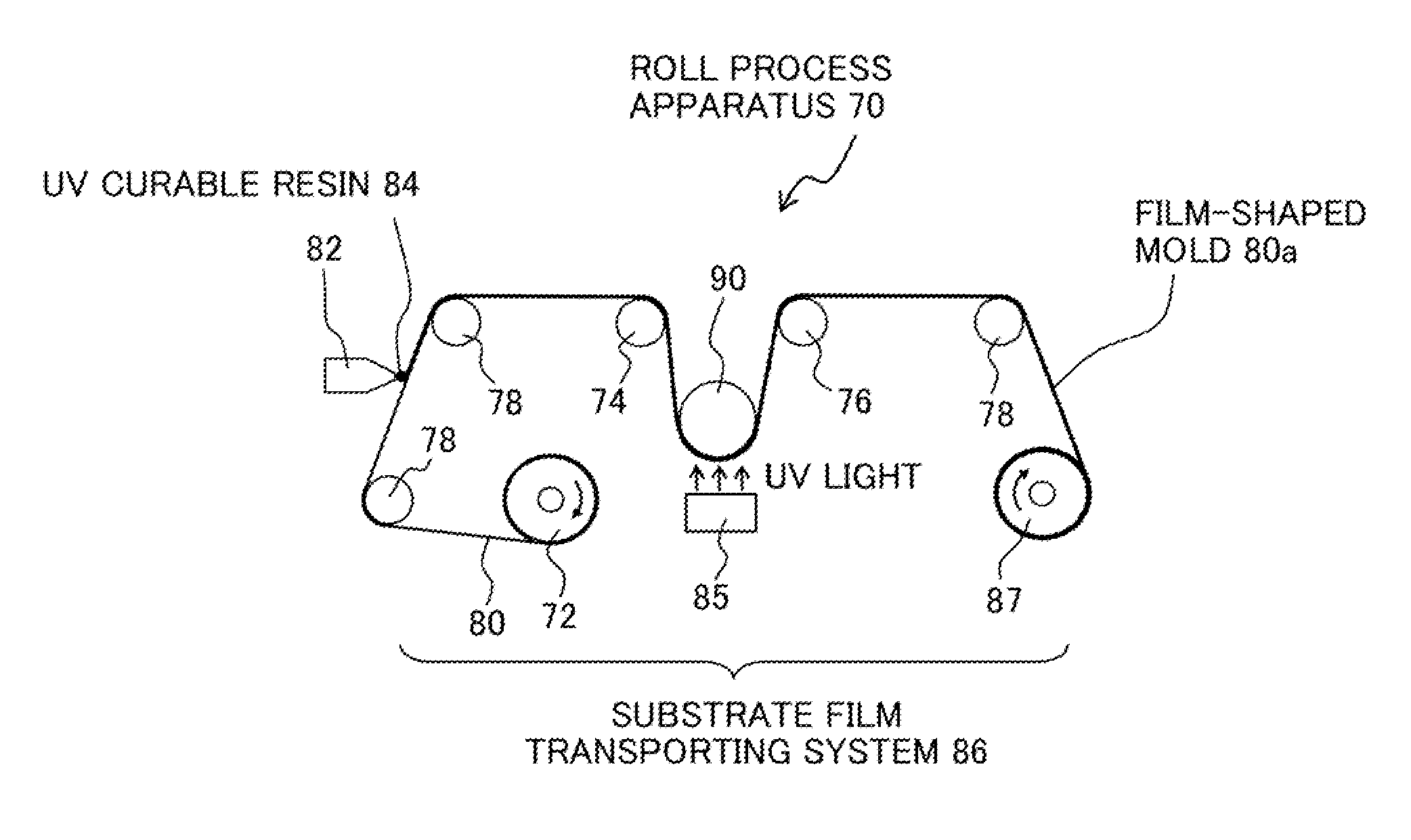
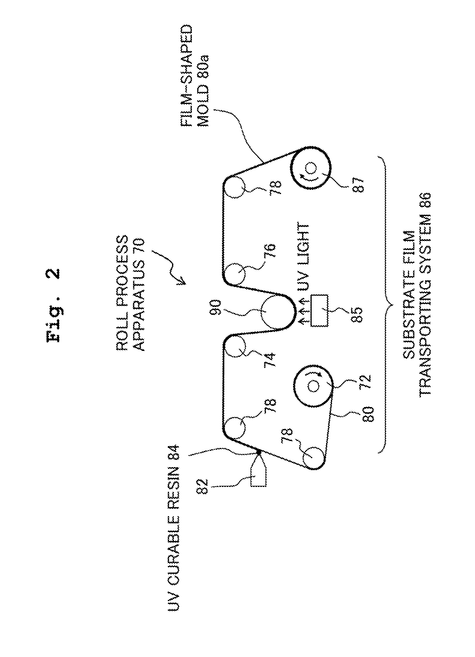
[0114]Although the peeling roll is provided on the optical substrate-producing apparatus 100 of the above-described embodiment, the peeling roll may be omitted as depicted in FIG. 5. In the apparatus depicted in FIG. 5, the film-shaped mold 80a fed from the mold feeding roll 21 (see FIG. 4) is pressed against the coating film 42 with a hot pressing roll 22, and then the film-shaped mold 80a is taken up or lifted with the mold take-up roll 24 (see FIG. 4) positioned above the substrate 40. By heating the pressing roll 22 and / or using any other heating means, the peeling (releasing) of the mold from the coating film immediately after the pressing is promoted and the pre-baking of the coating film can be performed.

second modification

[Second Modification]

[0115]In the optical substrate-producing apparatus 100 of the above-described embodiment, it is allowable to appropriately change the peeling angle (releasing angle) at which the film-shaped mold 80a is peeled (released) from the coating film 42 so as to further facilitate the peeling (releasing) of the film-shaped mold 80a from the coating film 42. For example, as depicted in FIG. 6, the peeling angle of the film-shaped mold 80a can be changed by the following manner. Namely, at first, the height at which the rotating rolls 36 are arranged is changed, at the releasing section 160, from the height at which the rotating rolls are arranged in the upstream of the releasing section 160 so as to incline the transporting direction of the substrate 40; further, in the releasing section 160, the arrangement position of the peeling roll 23 is changed in accordance with the inclination in the transporting direction of the substrate 40 so that the releasing rolls 23, the f...

third modification

[Third Modification]

[0116]Although the heater 22a is provided inside the pressing roll 22 in the optical substrate-producing apparatus 100 of the above-described embodiment, it is allowable to adopt a configuration as depicted in FIG. 7, instead of the configuration having the heater for heating the pressing roll 22. As depicted in FIG. 7, a heater 22b may be provided inside a heat zone 35 arranged at the periphery of the pressing roll 22 of the pressing section 150, rather than providing the heater inside the pressing roll 22. Since the heater is provided in the heat zone 35, the inside of the heat zone 35 is maintained at a heating temperature. In this case, the coating film 42 is subjected to the pre-baking in the heat zone 35. Note that the heater may be provided not only inside the heat zone 35 but also inside the pressing roll 22 and / or inside the supporting roll 26. Further, it is also allowable to provide several pieces of heating rolls, each of which has a heater provided t...


PUM

PropertyMeasurementUnit
Nanoscale particle sizeaaaaaaaaaa

Abstract

A method for producing an optical substrate includes: a step of preparing a long film-shaped mold having a concave-convex pattern surface having a concave-convex pattern; a step of forming a coating film made of a sol-gel material on the concave-convex pattern surface of the film-shaped mold; a step of adhering the coating film, which is formed on the concave-convex pattern surface of the film-shaped mold, to a substrate by arranging the concave-convex pattern surface of the film-shaped mold on which the coating film made of the sol-gel material is formed to face the substrate and by pressing a pressing roll against a surface of the film-shaped mold on a side opposite to the concave-convex pattern surface; a step of releasing the film-shaped mold from the coating film; and a step of curing the coating film adhered to the substrate.

Description

CROSS REFERENCE TO RELATED APPLICATION[0001]This application is a continuation application of International Patent Application No. PCT / JP2013 / 076791 filed on Oct. 2, 2013 claiming the benefit of priority of Japanese Patent Application No. 2012-223103 filed on Oct. 5, 2012. The contents of International Patent Application No. PCT / JP2013 / 076791 and Japanese Patent Application No. 2012-223103 are incorporated herein by reference in their entities.BACKGROUND OF THE INVENTION[0002]1. Field of the Invention[0003]The present invention relates to a producing method for producing an optical substrate having a minute or fine pattern for scattering or diffracting light, by using a long film-shaped mold (elongated or long-length film-shaped mold); and an apparatus performing the producing method.[0004]2. Description of the Related Art[0005]The lithography method is known as a method for forming a fine pattern (minute pattern) such as a semiconductor integrated circuit. The resolution of a patte...

Claims


Application Information

Patent Timeline
IPC IPC(8): B29D11/00G02B5/18G02B1/12G02B5/02
CPCB29D11/0073G02B5/0215B29L2011/00G02B1/12G02B5/0268G02B5/1852B29D11/00769B29C59/046G02B5/021B29D11/00326B29D11/00798Y10T428/24529H10K50/85
Inventor TORIYAMA, SHIGETAKANISHIMURA, SUZUSHIKOZASA, NAOTOTAKAHASHI, MADOKA
Owner JX NIPPON OIL & ENERGY CORP
Why Eureka
Try Eureka