Method for passivating surfaces, functionalizing inert surfaces, layers and devices including same

a technology of passivating surface and functionalizing inert surface, applied in the direction of semiconductor devices, basic electric elements, electrical apparatus, etc., can solve the problems of difficult to include 2d materials in device structures, difficult to grow oxides on graphene, and extremely unreactive 2d semiconductors such as graphene, and achieve the effect of high pressure processing

Active Publication Date: 2015-08-06
RGT UNIV OF CALIFORNIA
View PDF13 Cites 26 Cited by
  • Summary
  • Abstract
  • Description
  • Claims
  • Application Information

AI Technical Summary

Benefits of technology

[0011]An embodiment of the invention is a method for passivation of various surfaces (metal, polymer, semiconductors) from external contaminants, and the functionalization of inert surfaces. The method of the invention can functionalize 2D semiconductors and other insert surfaces such as non-reactive metals, oxides, insulators, glasses, and polymers. The method includes formation of a monolayer, an ordered bilayer or an ordered multilayer of metal phtha

Problems solved by technology

2D semiconductors such as graphene, boron nitride, and metal dichalcogenides (MDCs) are extremely un-reactive.
This presents challenges to including 2D materials in device structures.
The growth of oxides on graphene is also problematic.
Such non-uniformly grown oxide can create massive leakage currents in graphene based device.
This non-uniform oxide growth severely limits oxide scaling.
Fabricating conventional transistors with graphene is challenging because intrinsic graphene has zero band gap.
Due to this superfluidity, BiSFETs can be operated at a very low voltage, which in turn translates to low-power operation.
Commercially practical techniques have not yet

Method used


Image

  • Method for passivating surfaces, functionalizing inert surfaces, layers and devices including same
  • Method for passivating surfaces, functionalizing inert surfaces, layers and devices including same
  • Method for passivating surfaces, functionalizing inert surfaces, layers and devices including same

Examples


Embodiment Construction

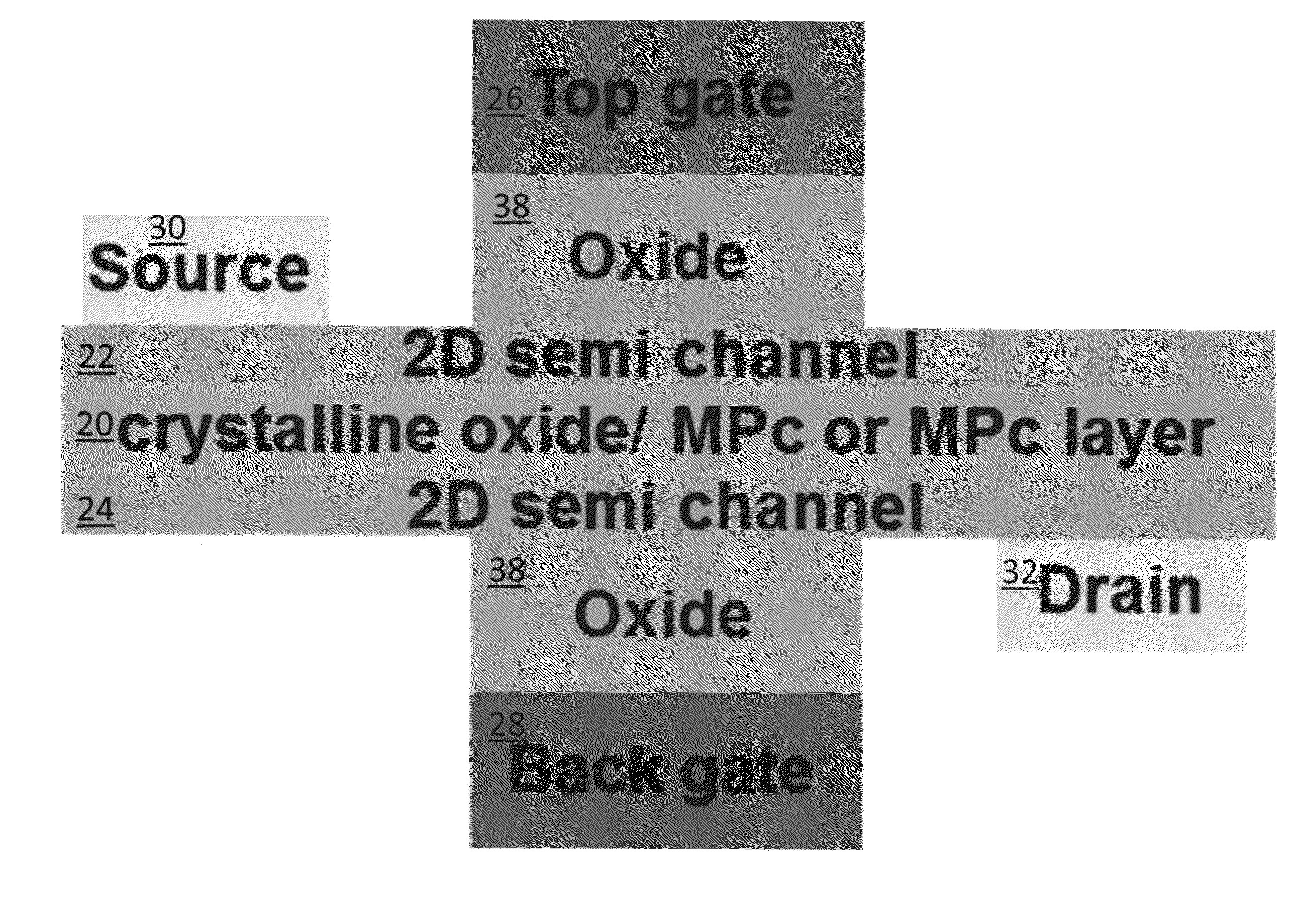
[0024]An embodiment of the invention is a method for passivation of various surfaces (metal, polymer, semiconductors) from external contaminants, and the functionalization of inert surfaces. The method of the invention can functionalize 2D semiconductor and other insert surfaces such as non-reactive metals, oxides, insulators, glasses, and polymers. The method includes formation of a monolayer, an ordered bilayer or an ordered multilayer of metal phthalocyanines (MPc).

[0025]The MPc can be TiOPc, AlOHPc, VOPc, FePc, CoPc, CuPc or other metal Pc, i.e. M is one of TiO, AlO, VO, Fe, Co, Cu or another metal ion or even a non-metal H2Pc. The MPc also includes crown-ether MPc. It is noted that although most of MPc molecules can be employed as coating materials, particularly preferred embodiments utilized polar MPc, such as TiOPc, VOPc, or AlOHPc. The polar MPc molecules have much higher reactivity for atomic layer deposition than non-polar MPc including FePc, CoPc CuPc, or H2Pc. In additio...


PUM


Abstract

The invention provides a method for passivation of various surfaces (metal, polymer, semiconductors) from external contaminants, and the functionalization of inert surfaces. The method of the invention can functionalize 2D semiconductor and other insert surfaces such as non-reactive metals, oxides, insulators, glasses, and polymers. The method includes formation of a monolayer, an ordered bilayer or an ordered multilayer of metal phthalocyanines (MPc). The invention also provides layer structure in a semiconductor device, the layer structure comprising one of an ordered monolayer, ordered bilayer or ordered multi-layer of metal phthalocyanine upon a surface, and one of an ALD deposited layer or 2D semiconductor on the one of a monolayer, ordered bilayer or ordered multi-layer of metal phthalocyanine.

Description

STATEMENT OF GOVERNMENT INTEREST[0001]This invention was made with government support under DARPA No. HR0011-13-30002 and NIST No. 70NANB12H107. The government has certain rights in the invention.FIELD[0002]A field of the invention is semiconductor devices and semiconductor device formation methods. Example applications of the invention include the passivation of various surfaces (metal, polymer, semiconductors) from external contaminants and functionalization of 2D semiconductor and other inert surfaces, such as non-reactive metals, oxides, insulators, glasses, and polymers for gate oxide atomic layer deposition, semiconductor atomic layer deposition, or metal contact deposition.BACKGROUND[0003]2D semiconductors such as graphene, boron nitride, and metal dichalcogenides (MDCs) are extremely un-reactive. This presents challenges to including 2D materials in device structures. Nucleation of any surface bonding either occurs only at defects, contaminants, or step edges or induced defe...

Claims


Application Information

Patent Timeline
IPC IPC(8): H01L21/02H01L29/16
CPCH01L21/0262H01L29/1606H01L21/02527H01L21/0254H01L21/0259H01L21/02118H01L21/02178H01L21/02318H01L21/02568H01L29/0673H01L21/0228H01L21/02304H10K85/311H10K10/486
Inventor PARK, JUN HONGKUMMEL, ANDREW C.
Owner RGT UNIV OF CALIFORNIA
Why Eureka
Try Eureka