Polymer Frame for a Chip, Such That the Frame Comprises at Least One Via in Series with a Capacitor

a polymer frame and capacitor technology, applied in the field of embedded chips, can solve the problems of high cost of manufacturing complex, low production efficiency, and inability to produce high-quality vias at a high density, and achieve the effects of enhancing reliability of rf (radio frequency) technologies, reducing manufacturing costs, and increasing production efficiency

Active Publication Date: 2015-08-13
ZHUHAI ADVANCED CHIP CARRIERS & ELECTRONICS SUBSTRATE SOLUTIONS TECH
View PDF7 Cites 59 Cited by
  • Summary
  • Abstract
  • Description
  • Claims
  • Application Information

AI Technical Summary

Benefits of technology

[0067]Optionally, a chip mounted in a socket is protected from electromagnetic radiation by a Faraday cage comprising via posts within the frame, thereby minimizing electromagnetic interference.
[0103]The combination of frames having inbuilt capacitors around chip sockets provides greater miniaturization, manufacturing economies and enhanced reliability for RF (Radio Frequency) technologies, such as Wi-Fi, Bluetooth and the like, which are widely used in mobile phones and automobiles, for example.

Problems solved by technology

There are a number of disadvantages with the drilled & filled via approach.
Since each via is required to be separately drilled, the throughput rate is limited, and the costs of fabricating sophisticated, multi-via IC substrates and interposers becomes prohibitive.
In large arrays it is difficult to produce a high density of high quality vias having different sizes and shapes in close proximity to each other by the drill & fill methodology.
This tapering reduces the effective diameter of the vias.
It may also adversely affect the electrical contact to the previous conductive metal layer—especially at ultra small via diameters, thereby causing reliability issues.
Additionally, the side walls are particularly rough where the dielectric being drilled is a composite material comprising glass or ceramic fibers in a polymer matrix, and this roughness may create additional stray inductances.
The electroplating deposition technique may result in dimpling, where a small crater appears at the top of the via.
Both dimpling and overfill tend to create difficulties when subsequently stacking vias one on top of the other, as required when fabricating high-density substrates and interposers.
Furthermore, it will be appreciated that large via channels are difficult to fill uniformly, especially when they are in proximity to smaller vias within the same interconnecting layer of the interposer or IC substrate design.
While the range of acceptable sizes and reliability is improving over time, the disadvantages described hereinabove are intrinsic to the drill & fill technology and are expected to limit the range of possible via sizes.
Although slot shaped via channels may theoretically be fabricated by laser milling, in practice, the range of geometries that may be fabricated is somewhat limited and vias in a given support structure are typically cylindrical and substantially identical.
Fabrication of vias by drill & fill is expensive and it is difficult to evenly and consistently fill the via channels created thereby with copper using the relatively, cost-effective electroplating process.
Laser drilled vias in composite dielectric materials are practically limited to diameters of 60×10−6 m (60 microns), and even so suffer from significant tapering and rough side walls due to the nature of the composite material drilled and in consequence of the ablation process involved.
In addition to the other limitations of laser drilling as described hereinabove, there is a further limitation of the drill & fill technology in that it is difficult to create different diameter vias in the same layer, since when drill different sized via channels are drilled and then filled with metal to fabricate different sized vias, the via channels fill up at different rates.
Consequently, the typical problems of dimpling or overfill that characterize drill & fill technology are exasperated, since it is impossible to simultaneously optimize deposition techniques for different sized vias.
Although the size of silicon wafers is growing, expensive material sets and manufacturing process are still limiting the wafer diameter size to 12″, thereby limiting the number of FOWLP units one can place on the wafer.
Despite the fact that 18″ wafers are under consideration, the investment required, materials sets and equipment are still unknown.
The limited number of chip support structures that may be processed at one time increases the unit cost of FOWLP, and make it too expensive for markets requiring highly competitive pricing, such as wireless communication, home appliances and automotive markets.
FOWLP also represents a performance limitation since the metal features placed over the silicon wafer as fan-out or fan-in circuitry are limited in thickness to a few microns.
This creates electrical resistance challenges.

Method used


Image

  • Polymer Frame for a Chip, Such That the Frame Comprises at Least One Via in Series with a Capacitor
  • Polymer Frame for a Chip, Such That the Frame Comprises at Least One Via in Series with a Capacitor
  • Polymer Frame for a Chip, Such That the Frame Comprises at Least One Via in Series with a Capacitor

Examples


Embodiment Construction

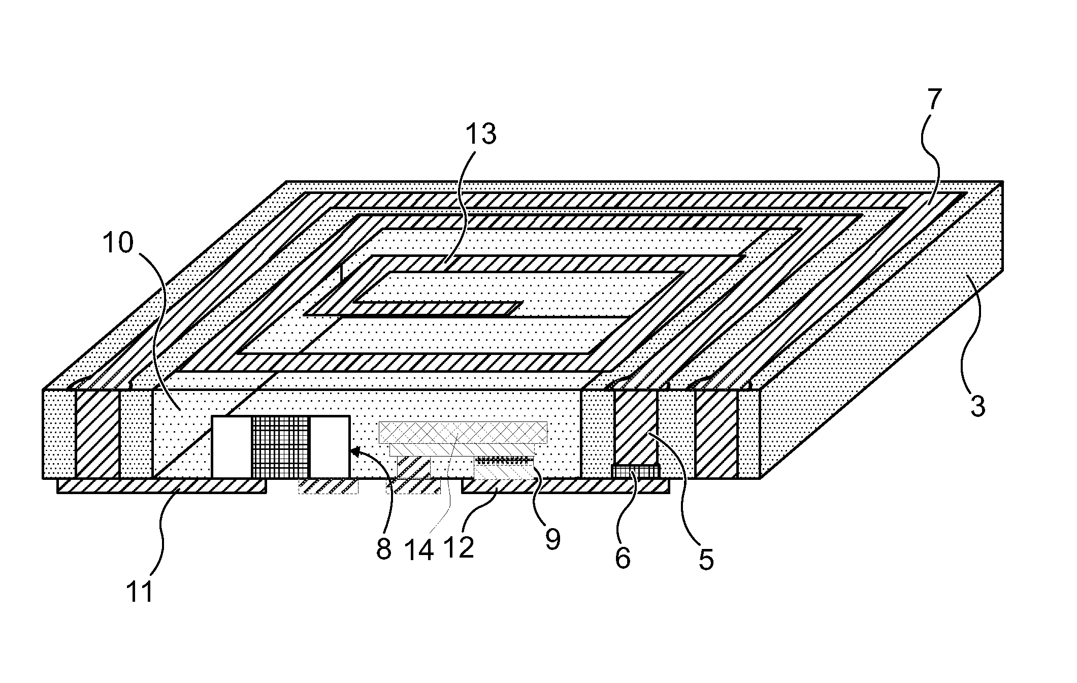
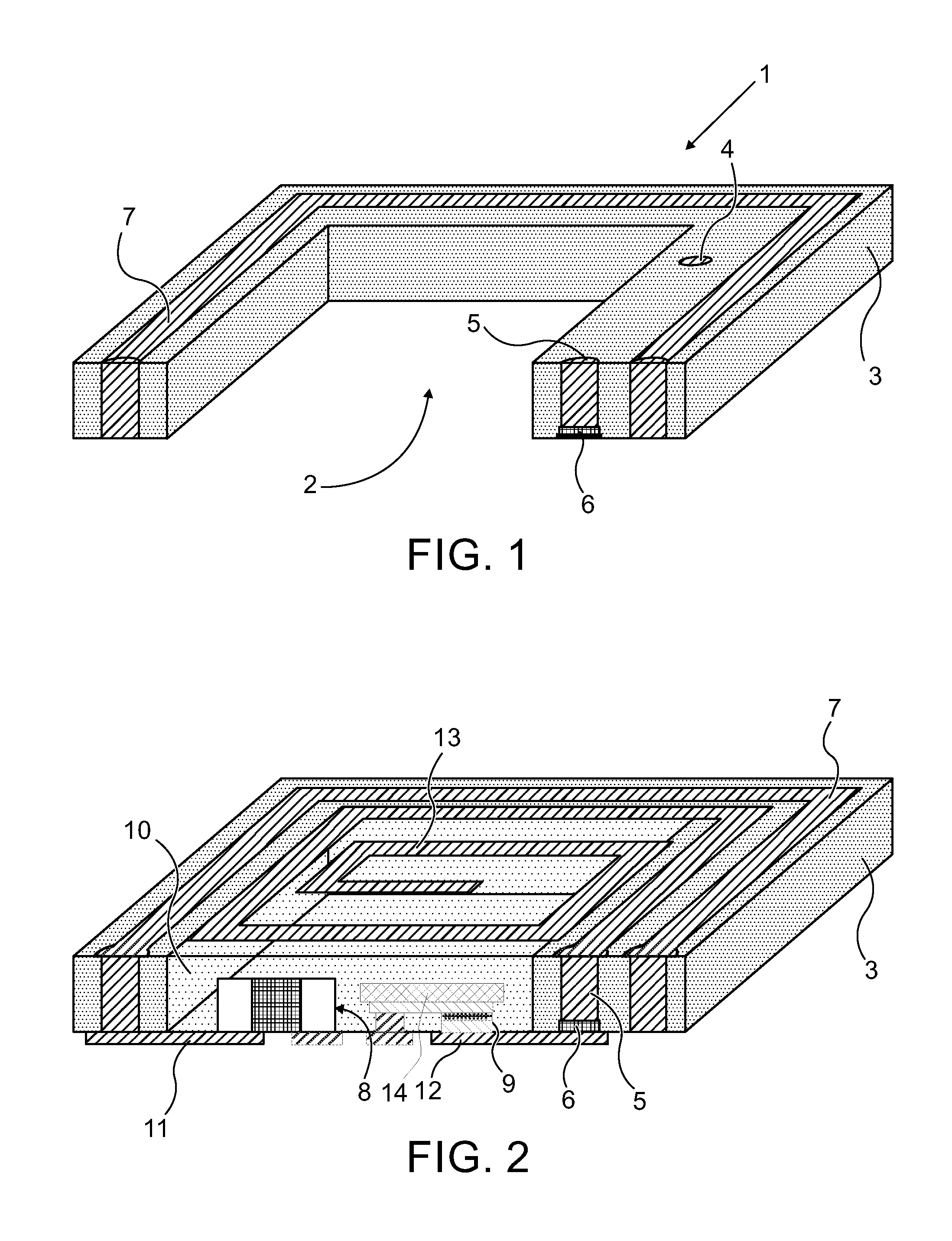
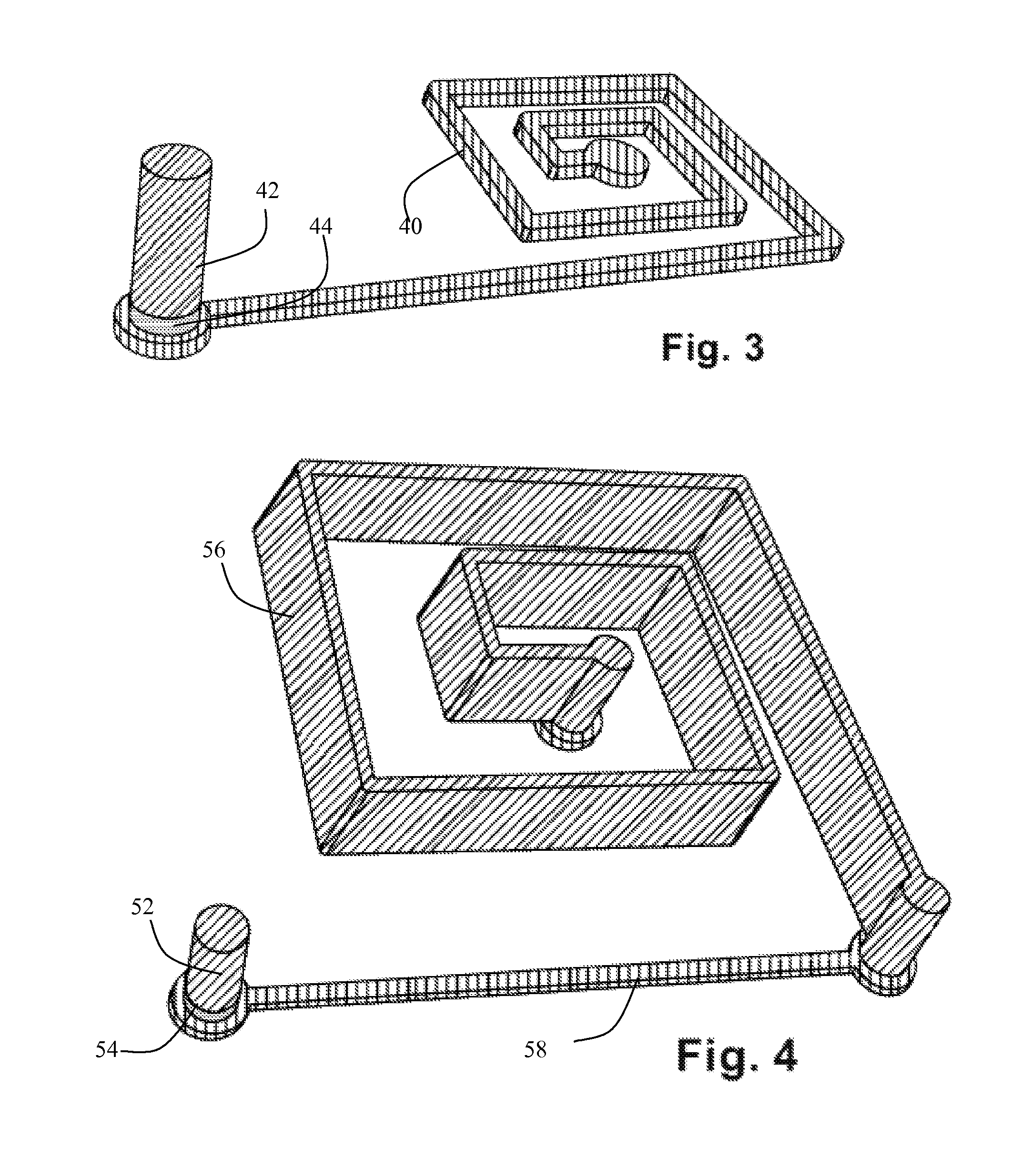
[0149]In the description hereinbelow, sockets structures for embedding chips are considered. The socket structures consist of metal vias in a dielectric matrix, particularly, copper via posts in a polymer matrix, such as polyimide, epoxy or BT (Bismaleimide / Triazine) or their blends, reinforced with glass fibers.

[0150]The socket structures described below further comprise capacitors built into the frame of the socket. Such capacitors are typically Metal Insulator Metal (M-I-M) Capacitors which comprises a lower metal electrode that may be gold, tantalum or tantalum, and an inorganic dielectric layer that may be Ta2O5, TiO2, BaxSr1-xTiO3, BaTiO3 or Al2O3, for example. The capacitor may comprise a dedicated upper electrode that is typically gold, tantalum or tantalum, or, the via, typically copper, may be deposited thereover as the upper electrode.

[0151]Since parallel plate capacitors comprise a dielectric material sandwiched between electrodes that is typically a material with a very...


PUM

PropertyMeasurementUnit
capacitanceaaaaaaaaaa

Abstract

A chip socket defined by an organic matrix framework, wherein the organic matrix framework comprises at least one via post layer where at least one via through the framework around the socket includes at least one capacitor comprising a lower electrode, a dielectric layer and an upper electrode in contact with the via post.

Description

[0001]The present invention claims priority from U.S. Ser. No. 13 / 962,075 to Hurwitz, filed on Aug. 8, 2013, and titled “Thin Film Capacitors Embedded in Polymer Dielectric”; from U.S. Ser. No. 13 / 962,316 to Hurwitz, filed on Aug. 8, 2013, and titled “Multilayer Structures and Embedded Features”, and from U.S. Ser. No. 14 / 269,884 to Hurwitz, filed of May 5, 2014 and titled “Interposer Frame With Polymer Matrix and Methods of Fabrication”.BACKGROUND[0002]1. Field of the Disclosure[0003]The present invention is directed to improved chip packaging and specifically to embedded chips wherewith passive components such as capacitors and filters are incorporated within the Chip package.[0004]2. Description of the Related Art[0005]Driven by an ever greater demand for miniaturization of ever more complex electronic components, consumer electronics such as computing and telecommunication devices are becoming more integrated. This has created a need for support structures such as IC substrates ...

Claims


Application Information

Patent Timeline
Patent Type & Authority Applications(United States)
IPC IPC(8): H01G17/00H05K1/18H05K1/11H03H7/01H01G4/008H05K1/02H01F27/28H05K1/16H01G4/12
CPCH01G17/00H05K2201/09609H05K1/181H05K1/182H05K1/115H01G4/1209H01G4/008H05K1/0222H05K1/0233H01F27/2804H03H7/0115H05K2201/10015H05K2201/1003H05K2201/0723H05K2201/10325H05K1/162H01G4/33H01G4/224H01G4/228H01L28/65H01L24/24H01L24/97H01L2224/24195H01L2924/19105H05K1/165H05K1/186H05K3/005H05K3/0052H05K3/4647H05K2201/09627H05K2201/09672H05K2201/098H05K2203/308H01L23/49822H01L23/49827H01L23/5389H01L2224/04105H01L2924/3025
Inventor HURWITZ, DRORHUANG, ALEX
Owner ZHUHAI ADVANCED CHIP CARRIERS & ELECTRONICS SUBSTRATE SOLUTIONS TECH
Why Eureka
Try Eureka