
Eureka
For R&D, Eureka makes reading and utilizing patents & technical documents easy.
Eureka AIR
Designed for self-driven R&D workflows. Generate viable solutions, solve complex R&D challenges, empower your innovation with AI.

Eureka Materials
Designed for material experts only. Revolutionize your material R&D, from search, analyze, to developing new materials.

TechResearch
Generate reliable direction feasibility study reports for your R&D in just a few steps.

TechSeek
Discover and master advanced knowledge NOW. Basics, ideas, possibilities, all at once.

TechMind
As an expert in R&D Theories, TechMind can generates customized viable solutions instantly.

TechRisk
Analyze your overall solution with one click, know your potential R&D risks in advance.

TechMonitor
Get weekly tech updates, stay abreast of the latest tech innovations and key insights.
Semiconductor structure having film including germanium oxide on germanium layer and method of fabricating the same
- Summary
- Abstract
- Description
- Claims
- Application Information
AI Technical Summary
Benefits of technology
Problems solved by technology
Method used
Image

Examples
first embodiment
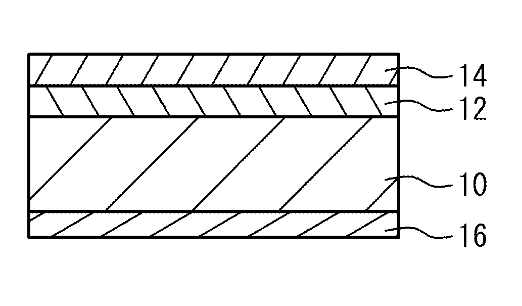
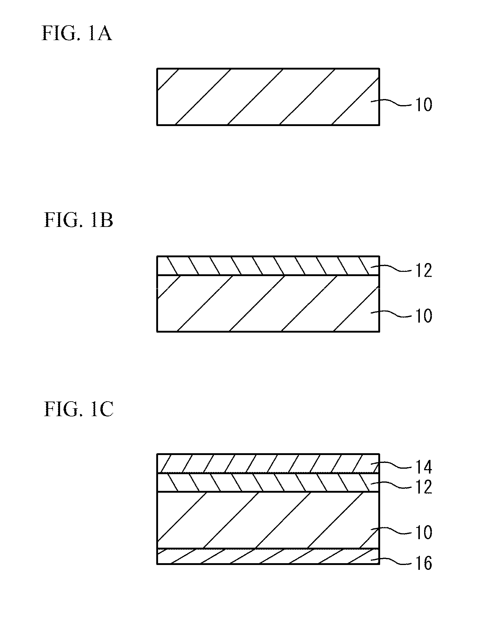
[0062]FIG. 8A and FIG. 8B illustrate cross sectional views for describing a fabricating method of a semiconductor structure in accordance with a first embodiment. As illustrated in FIG. 8A, a germanium layer 30 is prepared. The germanium layer 30 may be a single crystal germanium substrate or a germanium film formed on a substrate (for example, a silicon substrate). And, the germanium layer 30 may be a highly-pure germanium or may include an impurity. For example, the germanium layer 30 may be an n-type or a p-type germanium. Further, the germanium layer 30 may include some amounts of silicon that achieves the effect of the above-mentioned experiments. A composition ratio of the silicon may be 10 atomic % or less of the whole. A main face of the germanium layer 30 may be a (111) face or the like and may be another crystal face such as a (110) face or a (100) face.
[0063]As illustrated in FIG. 8B, a germanium oxide film 32 is formed on the germanium layer 30. The germanium oxide film ...
second embodiment
[0065]FIG. 9A to FIG. 9D illustrate cross sectional views for describing a fabricating method of a semiconductor structure in accordance with a second embodiment. As illustrated in FIG. 9A, the germanium layer 30 is prepared as described with respect to the first embodiment. As illustrated in FIG. 9B, a high dielectric oxide film 34 is formed on the germanium layer 30. The high dielectric oxide film 34 is a film having a dielectric constant higher than that of silicon oxide and is a film including at least one of a hafnium oxide film, a zirconium oxide film, an aluminum oxide film and an oxide film of a rare-earth element (for example, an yttrium oxide film or a scandium oxide film). For example, the high dielectric oxide film 34 may be one of the above-mentioned films or a film in which a plurality of above-mentioned films are laminated. The rare-earth element is scandium (Sc), yttrium (Y), lanthanum (La), cerium (Ce), praseodymium (Pr), neodymium (Nd), promethium (Pm), samarium (S...
PUM
 Abstract
Description
Claims
Application Information
 - R&D Engineer
- R&D Manager
- IP Professional
- Industry Leading Data Capabilities
- Powerful AI technology
- Patent DNA Extraction
Browse by: Latest US Patents, China's latest patents, Technical Efficacy Thesaurus, Application Domain, Technology Topic, Popular Technical Reports.
© 2024 PatSnap. All rights reserved.Legal|Privacy policy|Modern Slavery Act Transparency Statement|Sitemap|About US| Contact US: help@patsnap.com