Transparent quantum dot light-emitting diodes with dielectric/metal/dielectric electrode

a diode and quantum dot technology, applied in the direction of electroluminescent light sources, chemistry apparatus and processes, and compositions of light sources, can solve the problems of high fabrication cost, high cost of leds, and high current and heat management requirements, and achieve low sheet resistance and sufficient transparency

Active Publication Date: 2015-08-13
UNIV OF FLORIDA RES FOUNDATION INC
View PDF5 Cites 46 Cited by
  • Summary
  • Abstract
  • Description
  • Claims
  • Application Information

AI Technical Summary

Benefits of technology

[0010]The DMD electrode has a first particulate dielectric layer of 5 to 60 nm in thickness and a metal layer of about 5 to about 20 nm in thickness and is continuous so that it has a low sheet resistance yet is sufficiently transparent. The second dielectric layer is distal to the light emitting layer and can be either particulate or continuous.

Problems solved by technology

LEDs remain relatively expensive and require precise current and heat management relative to traditional light sources.
Fabrication costs are significant and exceed the material costs for some LEDs.
Another method is to use a yellow phosphor to convert monochromatic blue light, or two or more phosphors emitting different colors to convert UV light, from a LED to broad-spectrum white light, although color control is limited by this approach.
Organic LEDs (OLEDs) can also be fabricated relatively inexpensively to provide a variety of colors and white light, but OLEDs generally suffer from deficiencies in efficiency and in lifetime relative to inorganic devices as the light-emitting layer, being that of an organic material, typically requires a relatively high current density and driving voltage to achieve high luminance, which promotes degradation of the OLEDs, especially in the presence of oxygen, water and UV photons.
Unfortunately, long term stability is insufficient due to degradation of the organic layer and oxidation of the reactive metal.
Device fabrication requires a costly vacuum deposition method.
For most QD-LEDs, defects can occur at the organic-inorganic interface between the QD-emitting layer and an organic electron transport layer, which lead to poor electron injection into the QD-emitting layer.
However, the charge transporting layers are fabricated through complicated and costly vacuum sputter deposition methods.

Method used


Image

  • Transparent quantum dot light-emitting diodes with dielectric/metal/dielectric electrode
  • Transparent quantum dot light-emitting diodes with dielectric/metal/dielectric electrode
  • Transparent quantum dot light-emitting diodes with dielectric/metal/dielectric electrode

Examples


Embodiment Construction

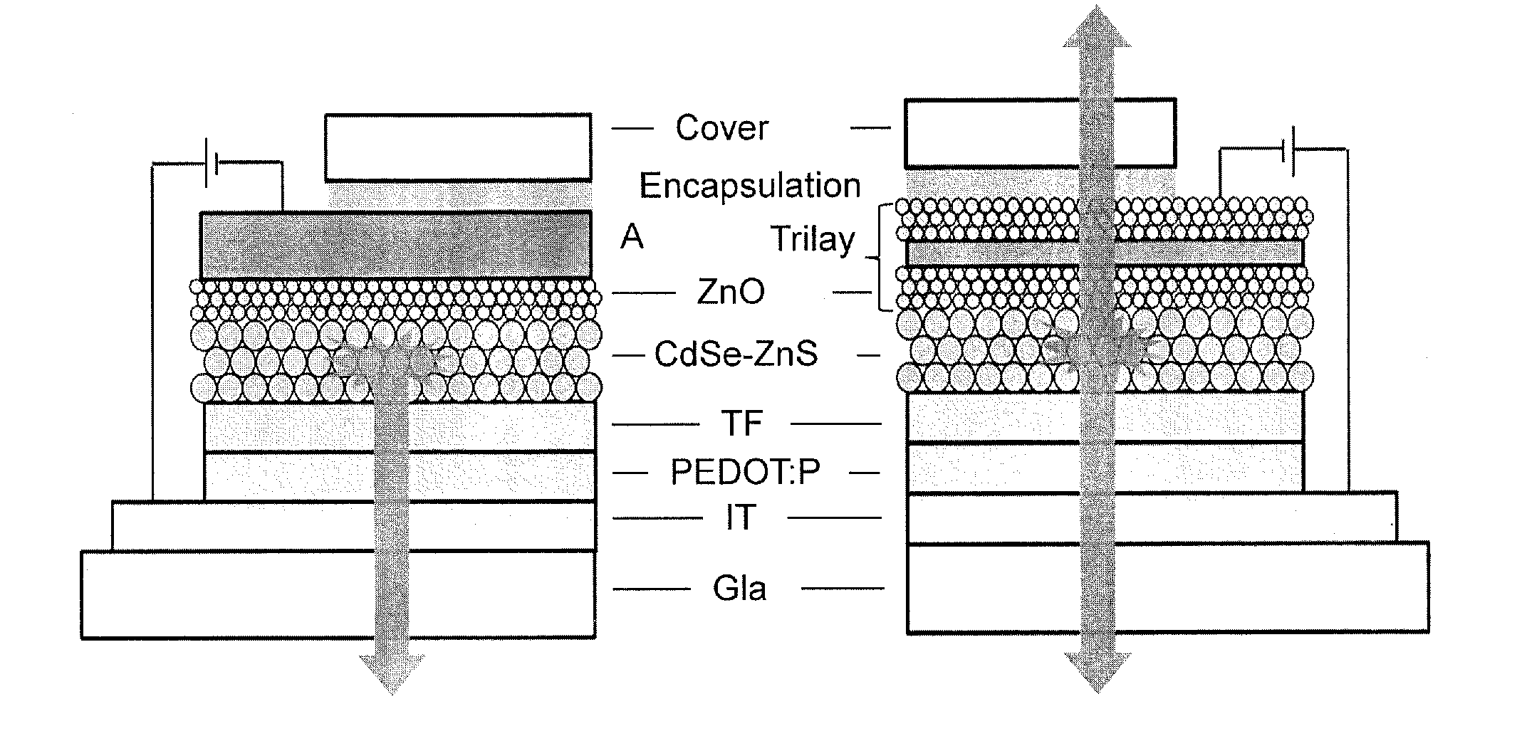
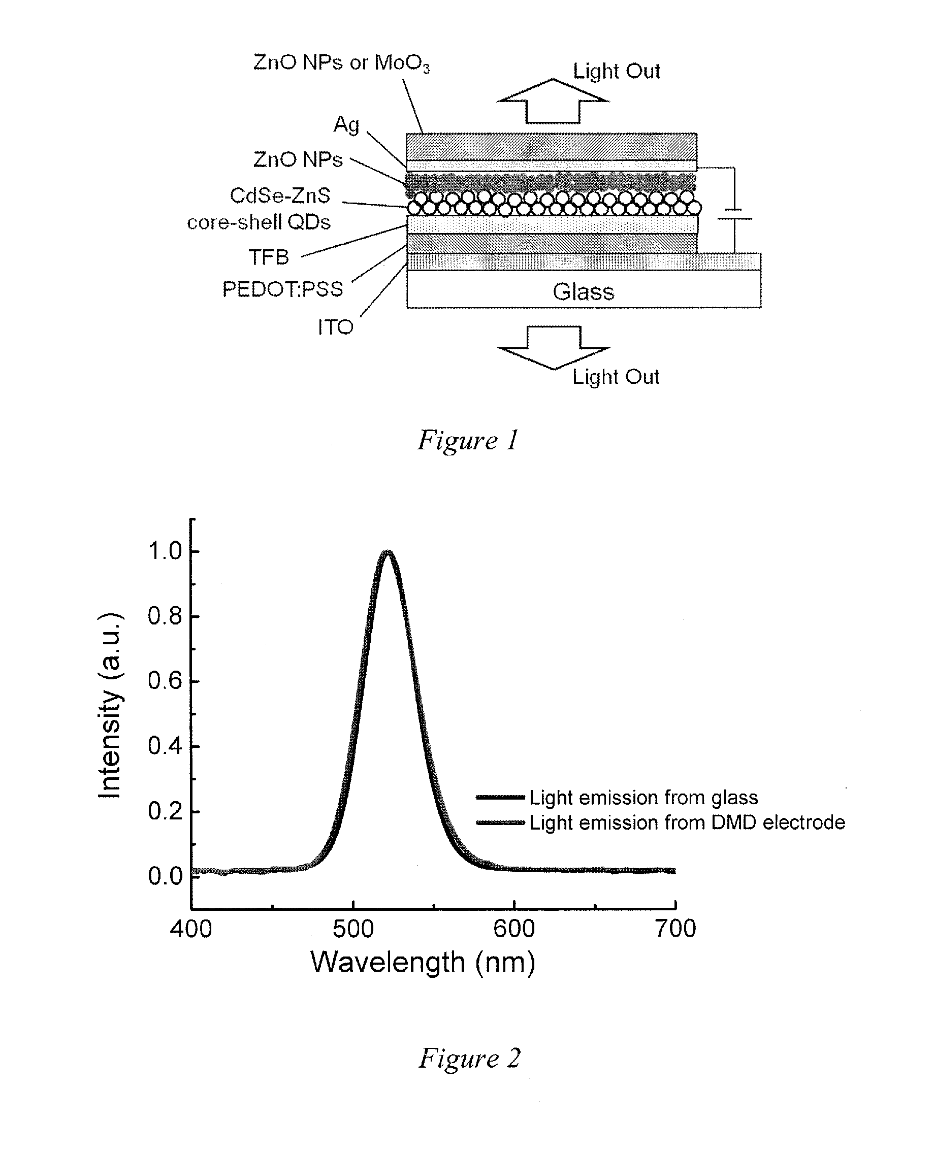
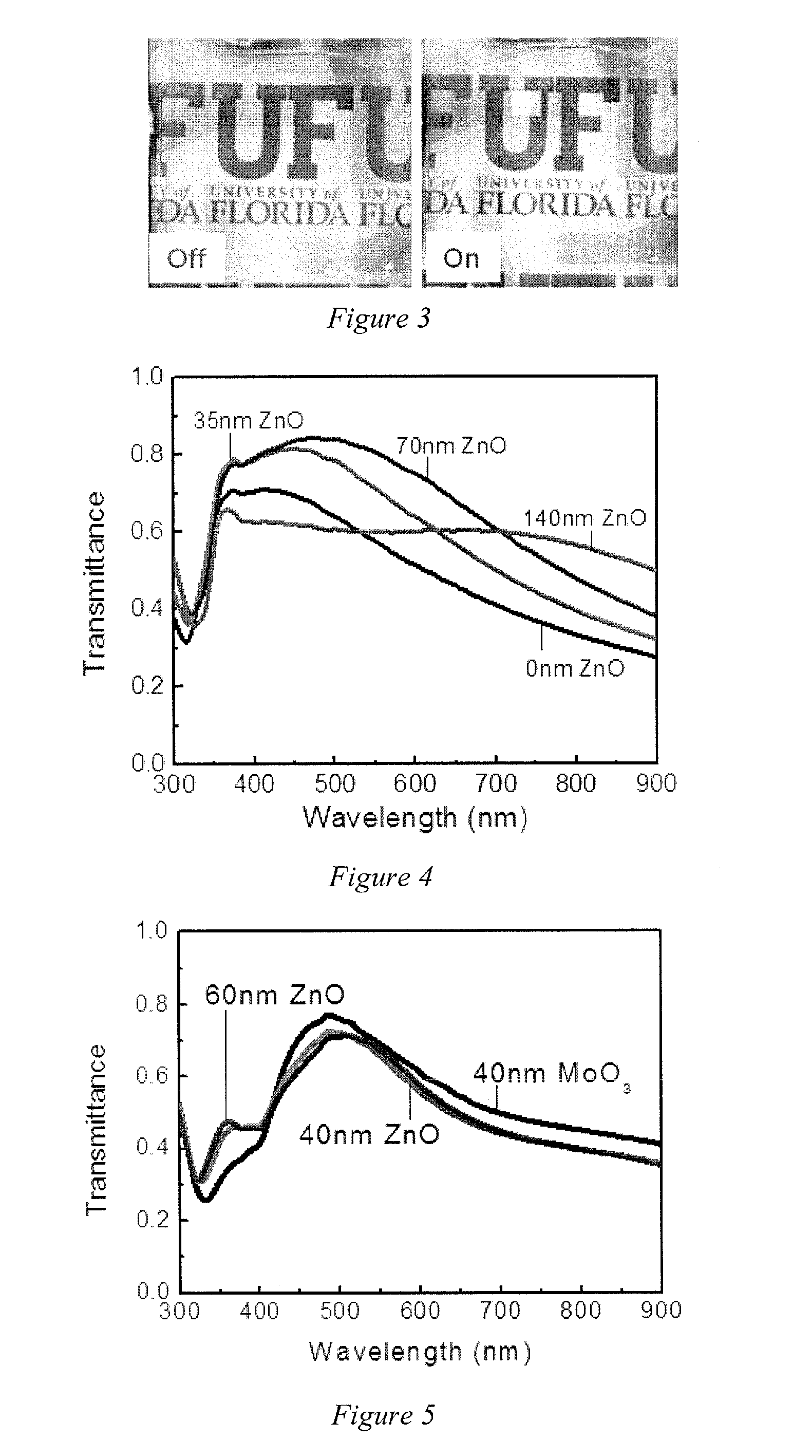
[0033]Embodiments of the invention are directed to transparent QD-LEDs that incorporate an electrode consisting of a layer of dielectric, a thin metal layer and an additional layer of dielectric, a DMD structure. Transparent QD-LEDs can be integrated with transparent display systems, owing to the high optical transparency of the thin QDs and carrier transport layers. Transparent QD-LEDs can be fabricated on the transparent windows of cars, airplanes and other facilities as the “head-up displays”. Transparent QD-LED panels can be integrated with house windows as innovative light systems, acting as normal windows during the daytime but transitioning to light sources after sunset. Transparent laptop and other such devices can be developed using these transparent QD-LEDs. The QD-LED employs the electrode with an dielectric / metal / dielectric (DMD) structure having an inner dielectric layer that serves the function of the charge transport and injection layer, whereas a thin metal layer, wi...


PUM

PropertyMeasurementUnit
thicknessaaaaaaaaaa
thicknessaaaaaaaaaa
thicknessaaaaaaaaaa

Abstract

Quantum dot light emitting diodes (QD-LEDs) are formed that are transparent and emit light from the top and bottom faces. At least one electrode of the QD-LEDs is a dielectric/metal/dielectric layered structure, where the first dielectric comprises metal oxide nanoparticles or polymer-nanoparticle blends and is 10 to 40 nm in thickness, the metal layer is 5 to 25 nm in thickness, and the second dielectric layer is a nanoparticulate, polymer-nanoparticle blend or continuous layer of 30 to 200 nm in thickness and is situated distal to the light emitting layer of the QD-LED.

Description

CROSS-REFERENCE TO RELATED APPLICATION[0001]The present application claims the benefit of of U.S. Provisional Application Ser. No. 61 / 705,676, filed Sep. 26, 2012, which is hereby incorporated by reference herein in its entirety, including any figures, tables, or drawings.[0002]This invention was made with government support under W911NF-07-0545 awarded by the Department of the Army. The government has certain rights in the invention.BACKGROUND OF INVENTION[0003]Light emitting diodes (LEDs) are increasingly used in modern display technologies. LEDs have many advantages over traditional light sources including: low energy consumption, long lifetime, robustness, small size and fast switching. LEDs remain relatively expensive and require precise current and heat management relative to traditional light sources. Fabrication costs are significant and exceed the material costs for some LEDs. Conventional LEDs are made from inorganic compound semiconductors, typically AlGaAs (red), AlGaInP...

Claims


Application Information

Patent Timeline
Patent Type & Authority Applications(United States)
IPC IPC(8): H01L33/06H01L33/00H01L33/30H01L33/28H01L33/26H01L33/08H01L33/40
CPCH01L33/06H01L33/08H01L33/002H01L33/305H01L33/285H01L33/26H01L33/40C09K11/565C09K11/883H05B33/14H05B33/22H05B33/26H10K85/115H10K85/1135H10K50/115
Inventor ZHENG, YINGCAO, WEIRANXUE, JIANGENGHOLLOWAY, PAUL H.
Owner UNIV OF FLORIDA RES FOUNDATION INC
Why Eureka
Try Eureka