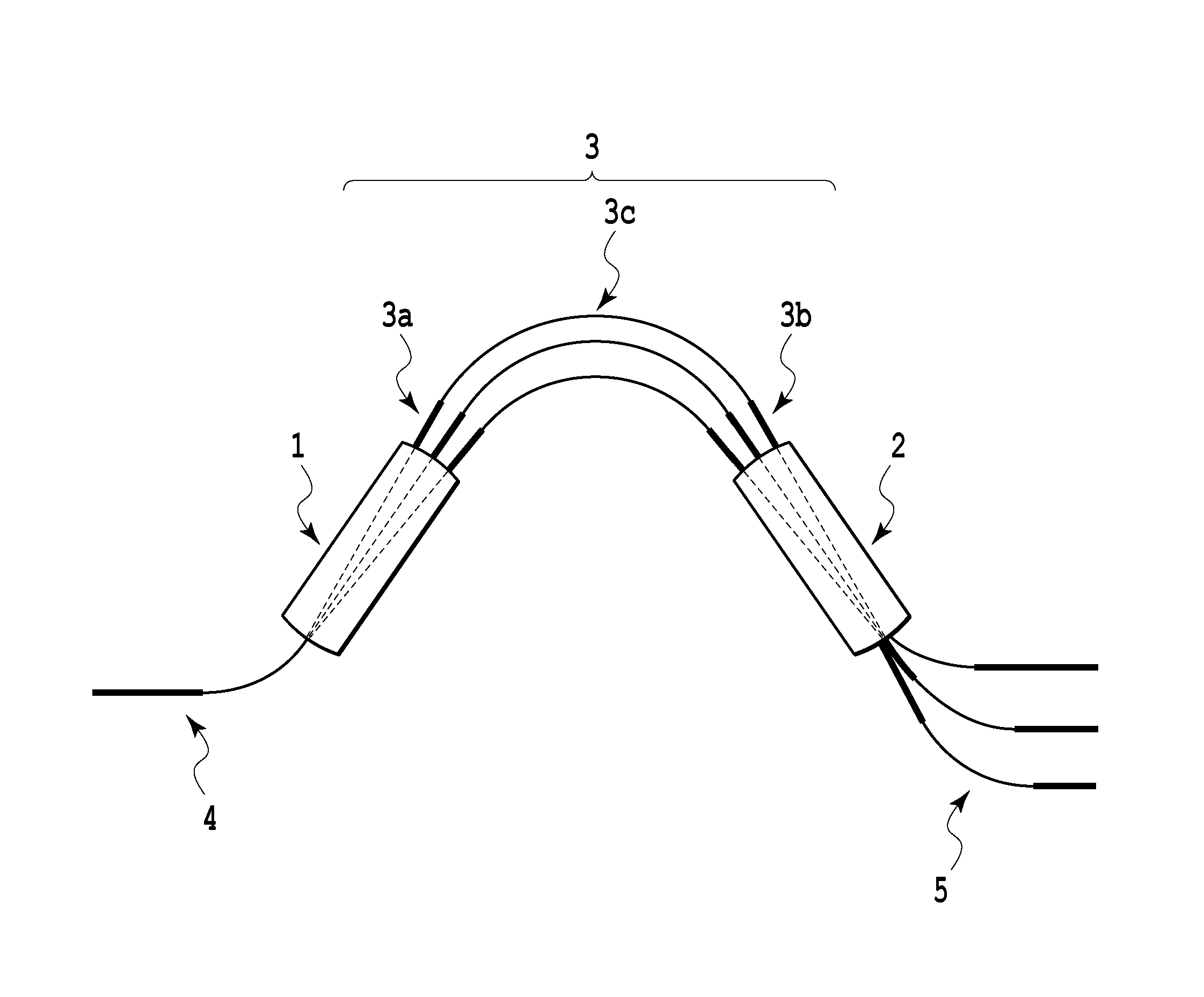
Optical multiplexer/demultiplexer

a multi-multi-plexer and optical technology, applied in multiplex communication, optical elements, instruments, etc., can solve the problems of increasing the capability of ethernet-based communication, increasing the difficulty of manufacturing optical modules using plurality of tffs, and unable to achieve easy reduction in size and cost. , to achieve the effect of reducing cost and high cos

Active Publication Date: 2015-08-13
NIPPON TELEGRAPH & TELEPHONE CORP
View PDF1 Cites 8 Cited by
  • Summary
  • Abstract
  • Description
  • Claims
  • Application Information

AI Technical Summary

Benefits of technology

[0026]The circuit size of the AWG main body can be reduced to some extent by increasing a refractive index difference (Δ) of the waveguide and decreasing a minimum bending radius; however, the size of an output fan-out part adapted to be coupled to individual PDs is also strongly dependent on a PD interval (or a terminal interval of TIAs connected to the PDs), and therefore there is a problem that sufficient miniaturization cannot be performed only by increasing Δ.
[0028]On the other hand, optical transceivers for Ethernet are supposed to be often used for connection in a data center and between data centers, and therefore compete with inexpensive electrical signal transceivers, so that the optical transceivers for Ethernet require a considerable reduction in cost as compared with optical transceivers for telecommunications.
[0029]An optical filter used for a ROSA should be, on the input side, optically coupled to a connector of an optical cable through an optical component called a receptacle, and on the output side, optically connected to four PDs through optical lenses. When assembling the ROSA, these components should be precisely aligned and fixed so as to prevent mutual misalignment.
[0030]The simplest method as an alignment method is one that makes light having an actually used signal light wavelength enter from the above-described optical cable, and pass sequentially through the optical filter, optical lenses, and PDs, and then while monitoring electrical outputs from the PDs, collectively performs multi-body alignment of all the components. However, this method requires a very complicated multi-body aligner, and therefore has a problem of extremely high cost.
[0031]Also, for a PD, optical filter, and optical fiber, different types of materials having very different refractive indices must be inevitably selected, and accordingly reflection at boundaries between the materials occurs. Further, in the case of using a lens system in order to increase coupling efficiency of each optical coupling, an air layer is added for each lens surface, and consequently reflection occurs many more times. To improve received S / N, typically, an antireflective film is provided for a telecommunication purpose; however, for an Ethernet purpose, a there is a challenge of avoiding an increase in cost along with the increase in processing step.
[0032]The present invention is made in consideration of the above-described conventional problems, and intends to provide a multiplexer / demultiplexer that can constitute a miniaturized, low-cost ROSA module necessary to realize high-speed Ethernet transceivers, and functions as an extremely small AWG optical filter. Further, another object is to suppress an increase in manufacturing cost of the ROSA module caused by a circuit added to the AWG optical filer, and the shape of a chip.Solution to Problem

Problems solved by technology

With the progress of the Internet, in particular, because of the expectation for progress in cloud computing, an increase in capability of Ethernet-based communication is an urgent challenge.
However, the optical module prepared using the plurality of TFFs becomes more difficult to manufacture with increasing the number of channels and reducing the size, and a reduction in size and a reduction in cost cannot be easily achieved at the same time.
However, the AWG had a problem once.
In the initial stage of AWG development, there was a problem that designing an AWG having a channel spacing of several 10 nm or more caused an increase in chip size.
In the case where a required wavelength interval is large, or a large number of channels are required, it is necessary to set the waveguide length difference d0 smaller; however, in the case where the waveguide length difference d0 is extremely small, in the arrayed waveguide group 3, an upper waveguide and a lower waveguide come into contact with or intersect with each other to make it difficult to appropriately operate the arrayed waveguide grating optical filter.
That is, according to the first conventional technique described above, from geometrical constraints, a settable waveguide length difference has a lower limit, and therefore the design method according to the first conventional example makes it geometrically impossible to set the optical path length difference extremely short, or even if the setting is possible, may anomalously increase the size of a circuit.
In the case of attempting to realize such a device as a waveguide type, the size of a usable substrate material has a certain limit, and accordingly in the case where the size of a circuit exceeds the certain limit, manufacturing such a device is substantially impossible.
Therefore, it is difficult for a wide FSR arrayed waveguide grating requiring setting an optical path length difference extremely short, i.e., an arrayed waveguide grating having a large wavelength interval at which multiplexing / demultiplexing is performed or an arrayed waveguide grating having a number of channels to employ such a configuration.
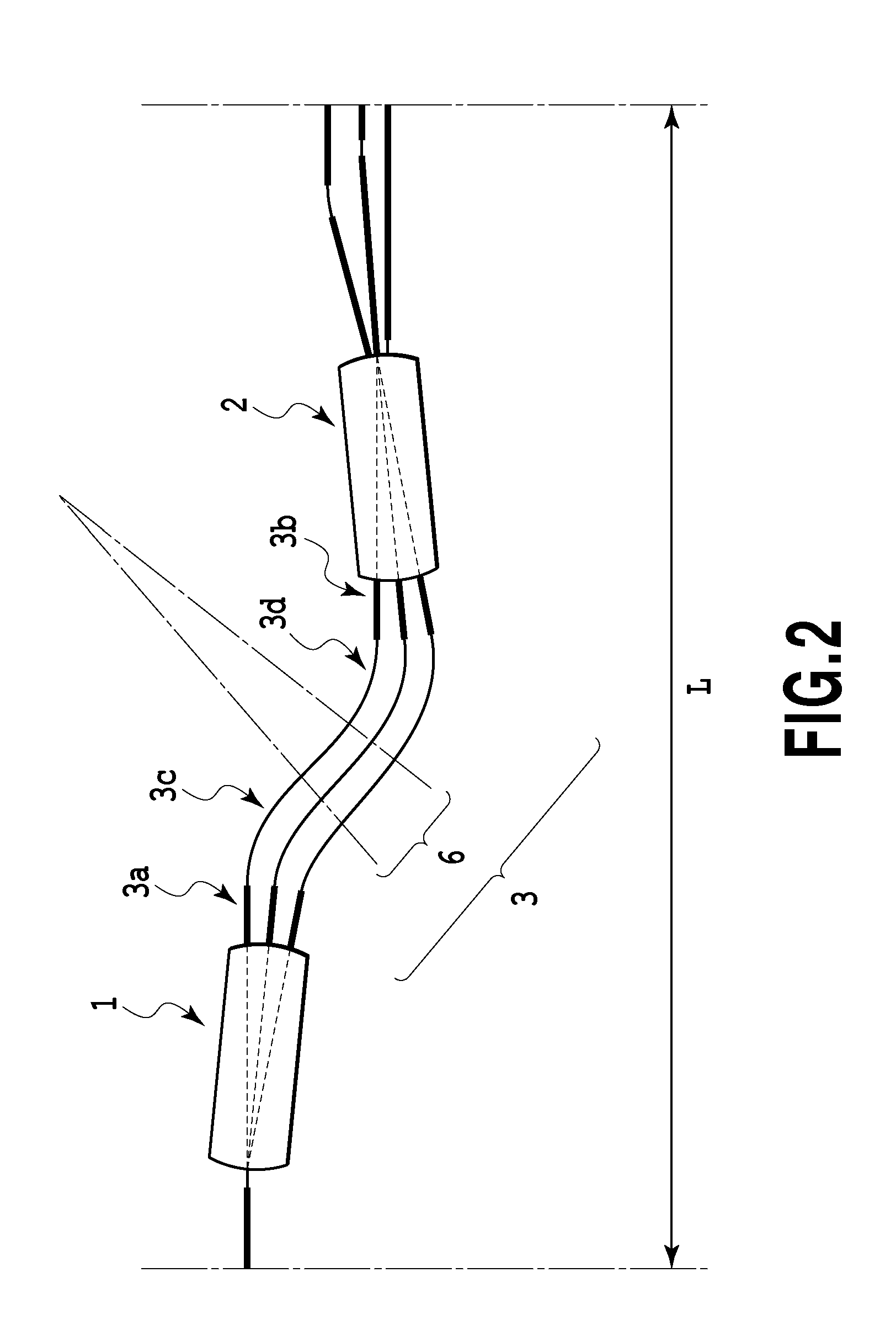
On the other hand, the configuration as illustrated in FIG. 2 gives rise to a problem that the waveguide is point symmetrically arranged on the basis of the S-shaped structure, and therefore the length L of the circuit is large.
As a result, there is a problem that the size of the circuit exceeds the size of an effective substrate, or even in the case where the circuit can be arranged on the substrate, the number of circuits arrangeable on one substrate is small.
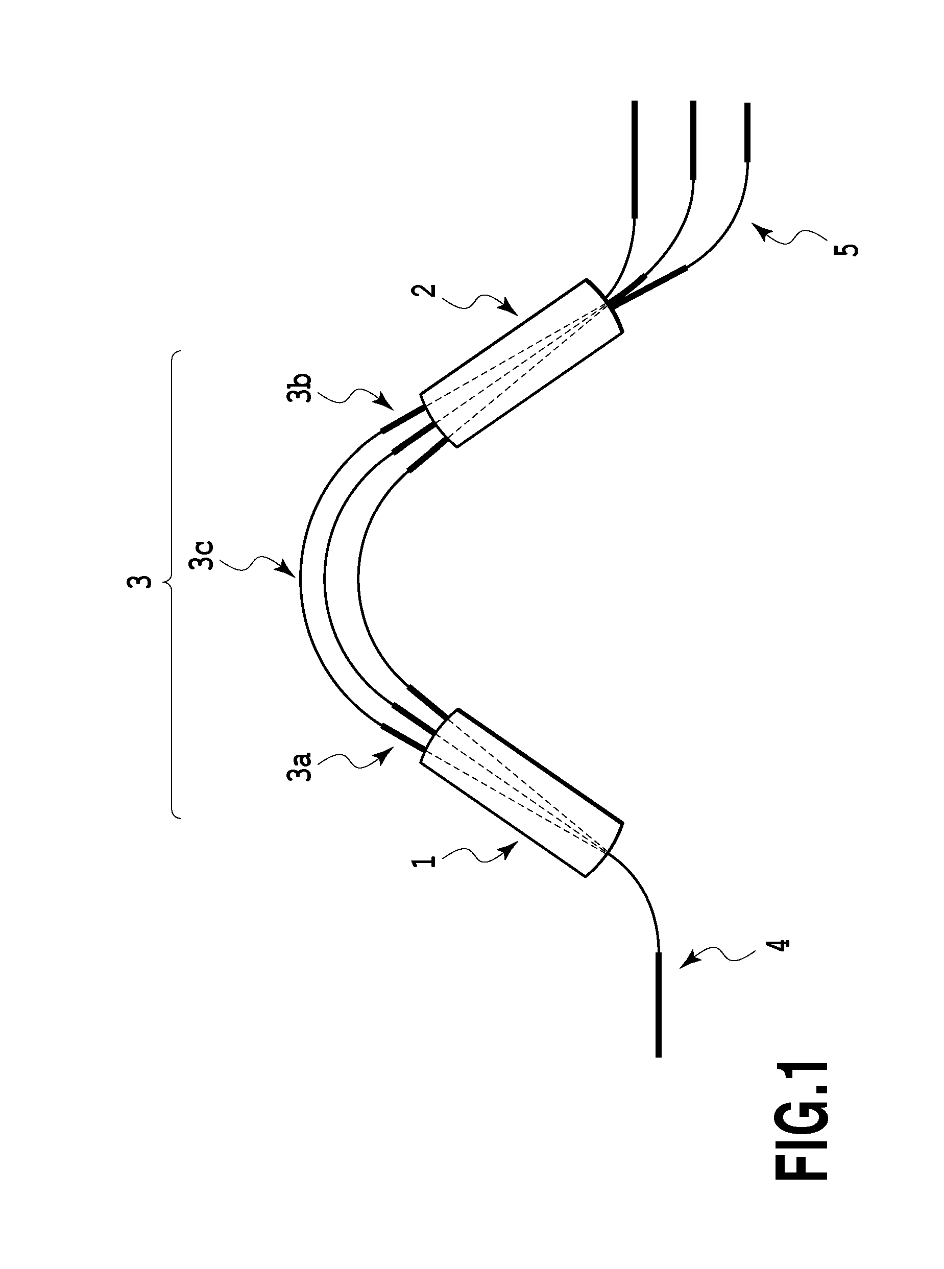
However, protruding directions of arcs of the arcuate waveguides 3c and arcuate waveguides 3d are all upward, and therefore relative to a lower waveguide, an upper waveguide is inevitably long.

Method used


Image

  • Optical multiplexer/demultiplexer
  • Optical multiplexer/demultiplexer
  • Optical multiplexer/demultiplexer

Examples


first example

[0059]FIG. 4 illustrates the outline of an arrayed waveguide grating optical filter according to this example. As illustrated in FIG. 4, the arrayed waveguide grating optical filter according to this example includes a first slab waveguide 11, second slab waveguide 12, arrayed waveguide group 13, input waveguide 14, and output waveguides 15.

[0060]The arrayed waveguide group 13 is an arrayed waveguide group including S-shaped waveguides respectively configured by connecting linear waveguide 13a, arcuate waveguides 13b, arcuate waveguides 13c, linear waveguides 13d, arcuate waveguides 13e, arcuate waveguides 13f, first waveguide length difference adjusting linear waveguides 17a, arcuate waveguides 13g, linear waveguides 13h, arcuate waveguides 13i, second waveguide length difference adjusting linear waveguides 17b, arcuate waveguides 13j, and linear waveguides 13k in series, and the total length of each of the S-shaped waveguides monotonously increases or decreases by a constant value...

second example

[0080]In this example, in order to make the arrayed waveguide grading optical multiplexer / demultiplexer in the first example function as an aligning waveguide-equipped arrayed waveguide grating optical filter for LAN-WDM signal demultiplexing, the arrayed waveguide grating optical multiplexer / demultiplexer is configured such that wavelengths of optical signals to be demultiplexed are different. FIG. 8 is a waveguide arrangement diagram of the aligning waveguide-equipped arrayed waveguide grating optical filter for LAN-WDM signal demultiplexing designed in this example. Materials for waveguides and waveguide parameters used are the same as those of the arrayed waveguide grating optical multiplexer / demultiplexer illustrated in FIG. 5; however, wavelengths of optical signals to be demultiplexed are different. The wavelengths of the four waves were set to 1295.56 nm, 1300.05 nm, 1304.58 nm, and 1309.14 nm, and in consideration of a difference in transmission loss between channels, an FS...


PUM


Abstract

A multiplexer / demultiplexer that functions as an extremely small AWG optical filter in order to prepare a miniaturized and low-cost transceiver module necessary to realize a high speed transceiver for Ethernet (registered trademark). An optical multiplexer / demultiplexer includes: at least one input waveguide, a first slab waveguide, an arrayed waveguide group, a second slab waveguide, and at least one output waveguide. Each of the waveguides of the arrayed waveguide group has: a first bent part of which a waveguide extending direction changes 180 degrees or more; and a second bent part of which a waveguide extending direction changes 180 degrees or more in a direction opposite to a direction of the change of the first bent part.

Description

TECHNICAL FIELD[0001]The present invention relates to an optical multiplexer / demultiplexer that functions as an optical filter for a miniaturized optical transceiver adapted to make optical communication. More specifically, the present invention relates to an optical multiplexer / demultiplexer that is used for an optical communication device necessary for connection in a data center or between data centers.BACKGROUND ART[0002]With the progress of the Internet, in particular, because of the expectation for progress in cloud computing, an increase in capability of Ethernet-based communication is an urgent challenge. As the next-generation high-speed 40 G / 100 G Ethernet (registered trademark) standard, IEEE 802.3ba (NPL 1) was released in 2010, and discussions have been made. In particular, the range of several tens m to several tens km in transmission distance corresponds to a distance necessary for connection in a data center or between data centers, and is focused on because of large...

Claims


Application Information

Patent Timeline
Patent Type & Authority Applications(United States)
IPC IPC(8): H04B10/40H04J14/02
CPCH04J14/02H04B10/40G02B6/12011G02B6/12021G02B6/12
Inventor OGUMA, MANABUOGAWA, IKUODOI, YOSHIYUKIITOH, MASAYUKITAKAHASHI, HIROSHI
Owner NIPPON TELEGRAPH & TELEPHONE CORP
Why Eureka
Try Eureka