Distortion compensation circuit and transmission device using distortion compensation circuit and high-frequency power amplifier

a distortion compensation circuit and distortion compensation technology, applied in the direction of high-frequency amplifiers, digital transmission, amplifier modifications to reduce non-linear distortion, etc., can solve the problems of reducing the power supply efficiency of the amplifier, requiring time for convergence of the pre-compensation for reducing the even order distortion of the memory effect, and extremely short peak power produced

Active Publication Date: 2015-08-20
KOKUSA ELECTRIC CO LTD
View PDF5 Cites 12 Cited by
  • Summary
  • Abstract
  • Description
  • Claims
  • Application Information

AI Technical Summary

Benefits of technology

[0034]As described above, according to the present invention, the Cartesian loop transmission delay can be made shorter than the time constant of the memory effect and the even order distortion of the memory effect produced by the power amplifier can be compensated to converge the compensation in a short time.

Problems solved by technology

When the linearity is ensured by supplying a power amplifier with such a fixed voltage as to be able to produce peak power in a power amplification system, the time that the peak power is produced is extremely short and as a result the power supply efficiency of the amplifier is reduced.
However, the techniques for compensating the even order distortion by the differentiation of amplitude and phase in the patent literatures 2 and 3 have a drawback that convergence of the pre-compensation for reducing the even order distortion of the memory effect requires time even if the even order distortion of the memory effect is changed.
However, input / output and wiring of a chip are contained in a path for the feedback and accordingly transmission of signals is delayed for that.
Influence of this delay is increased in proportion to frequency and accordingly there arises a problem that the stability is deteriorated when the band is widened.
In the non-patent literature 6, a complicated analog feedback path is added, so that it is difficult to make application to large-power amplification.

Method used


Image

  • Distortion compensation circuit and transmission device using distortion compensation circuit and high-frequency power amplifier
  • Distortion compensation circuit and transmission device using distortion compensation circuit and high-frequency power amplifier
  • Distortion compensation circuit and transmission device using distortion compensation circuit and high-frequency power amplifier

Examples


embodiment 1

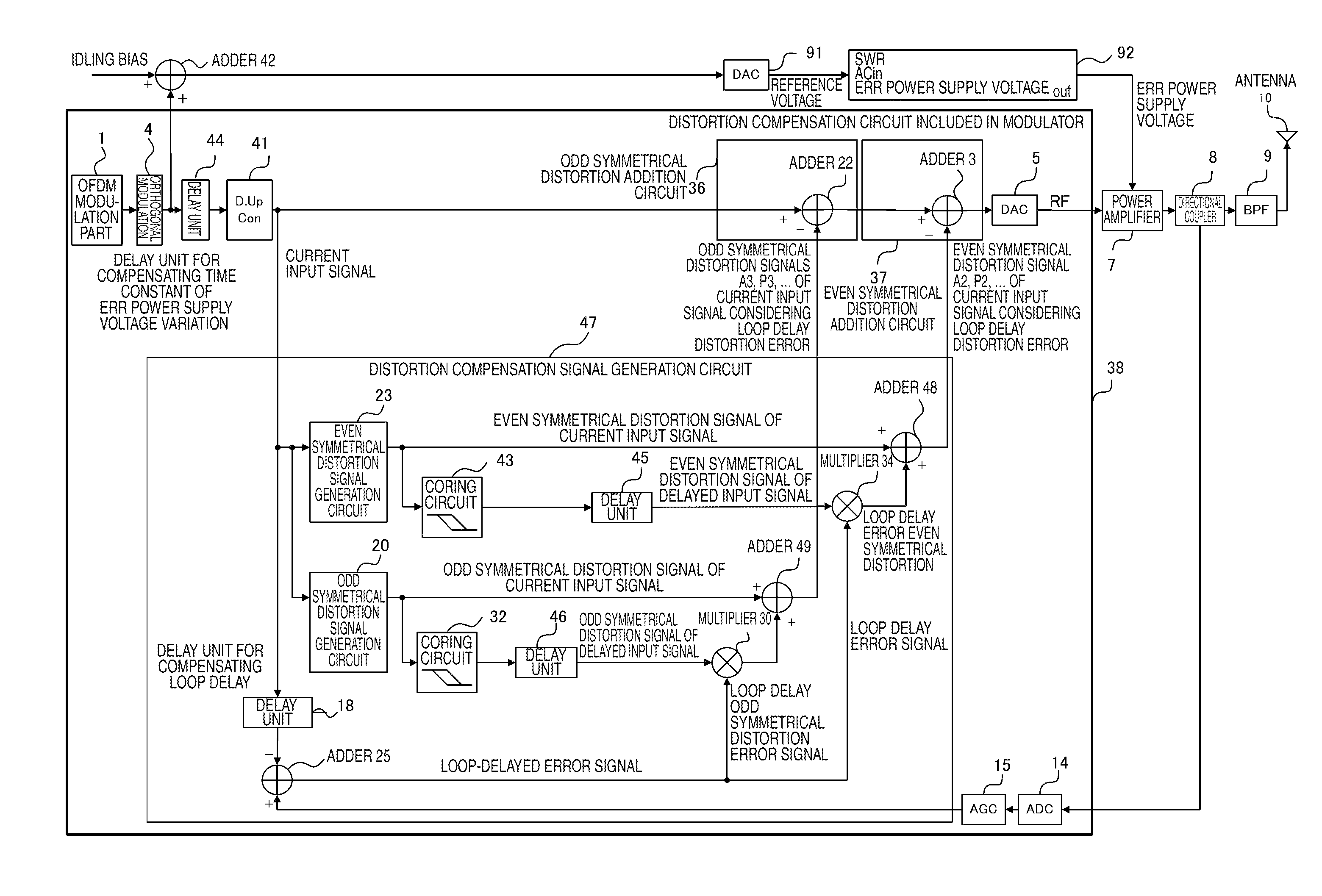
[0052]Configuration and operation of an embodiment of the present invention are now described referring to FIG. 1A schematically illustrating in a block diagram a transmitter of the embodiment of the present invention (digital frequency conversion of a digital up converter and a digital down converter, a high-frequency band ADC and a high-frequency band DAC for making compensation after orthogonal modulation), FIG. 2 illustrating in a block diagram an odd symmetrical distortion signal generation circuit in the embodiment of the present invention, FIG. 3 illustrating in a block diagram an even symmetrical distortion signal generation circuit in the embodiment of the present invention, FIG. 4A schematically illustrating a time constant of the memory effect distortion of a high-frequency power amplifier, a time constant of a Cartesian loop of distortion compensation in comparison of baseband input signals and an OFDM baseband input signal, FIG. 4B schematically illustrating envelope de...

embodiment 2

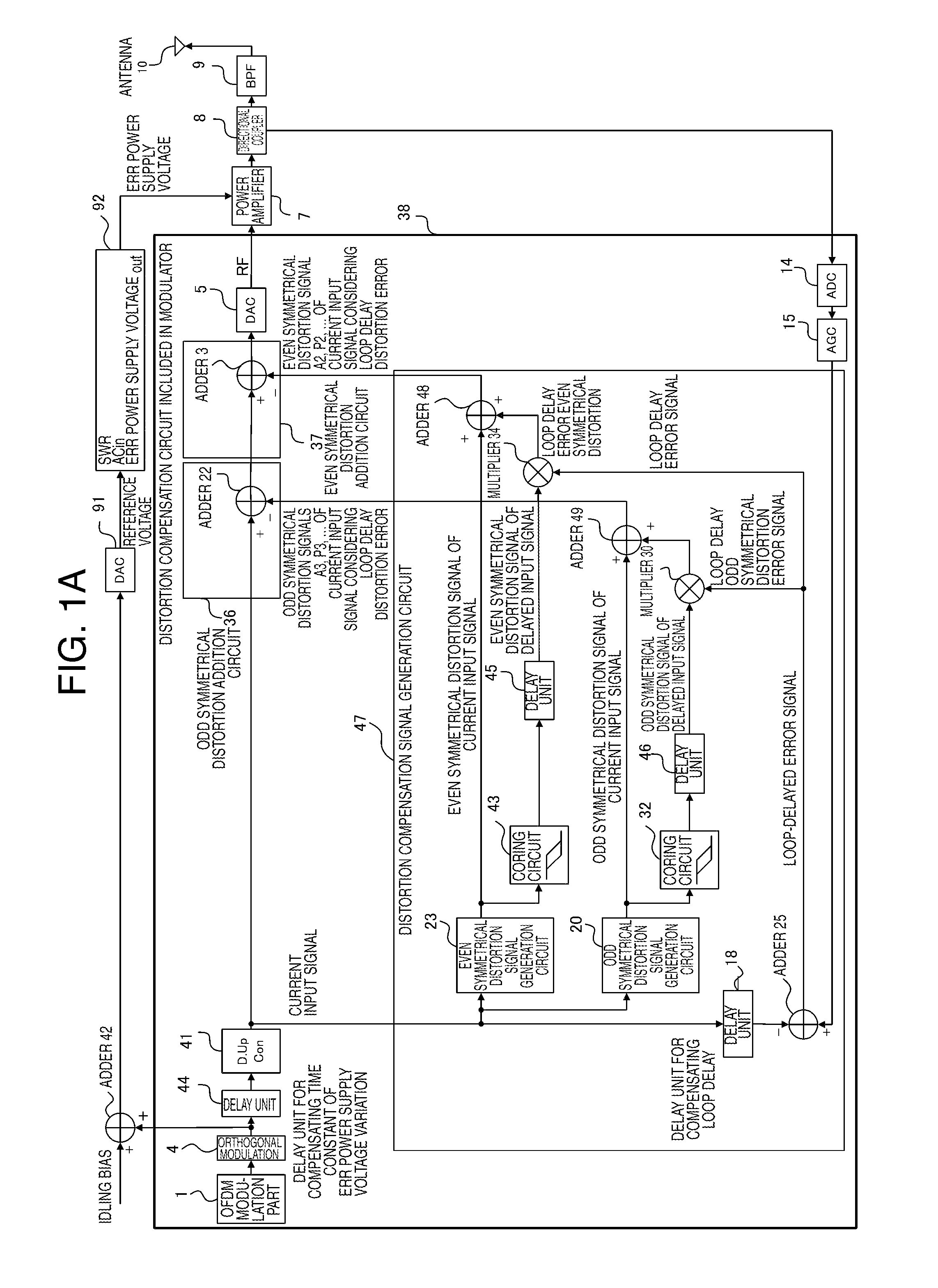
[0068]Next, an embodiment 2 is described. Description of the same configuration and operation as the embodiment 1 is omitted and only different points are described.

[0069]Description of configuration and operation of the embodiment of the present invention is made referring to FIG. 1B illustrating in a block diagram the transmitter (orthogonal compensation ADC and orthogonal compensation DAC after orthogonal modulation) of the embodiment of the present invention instead of FIG. 1A illustrating in a block diagram the transmitter (digital frequency conversion, high-frequency band ADC and high-frequency band DAC of a digital up converter and a digital down converter in compensation after orthogonal modulation) of the embodiment of the present invention.

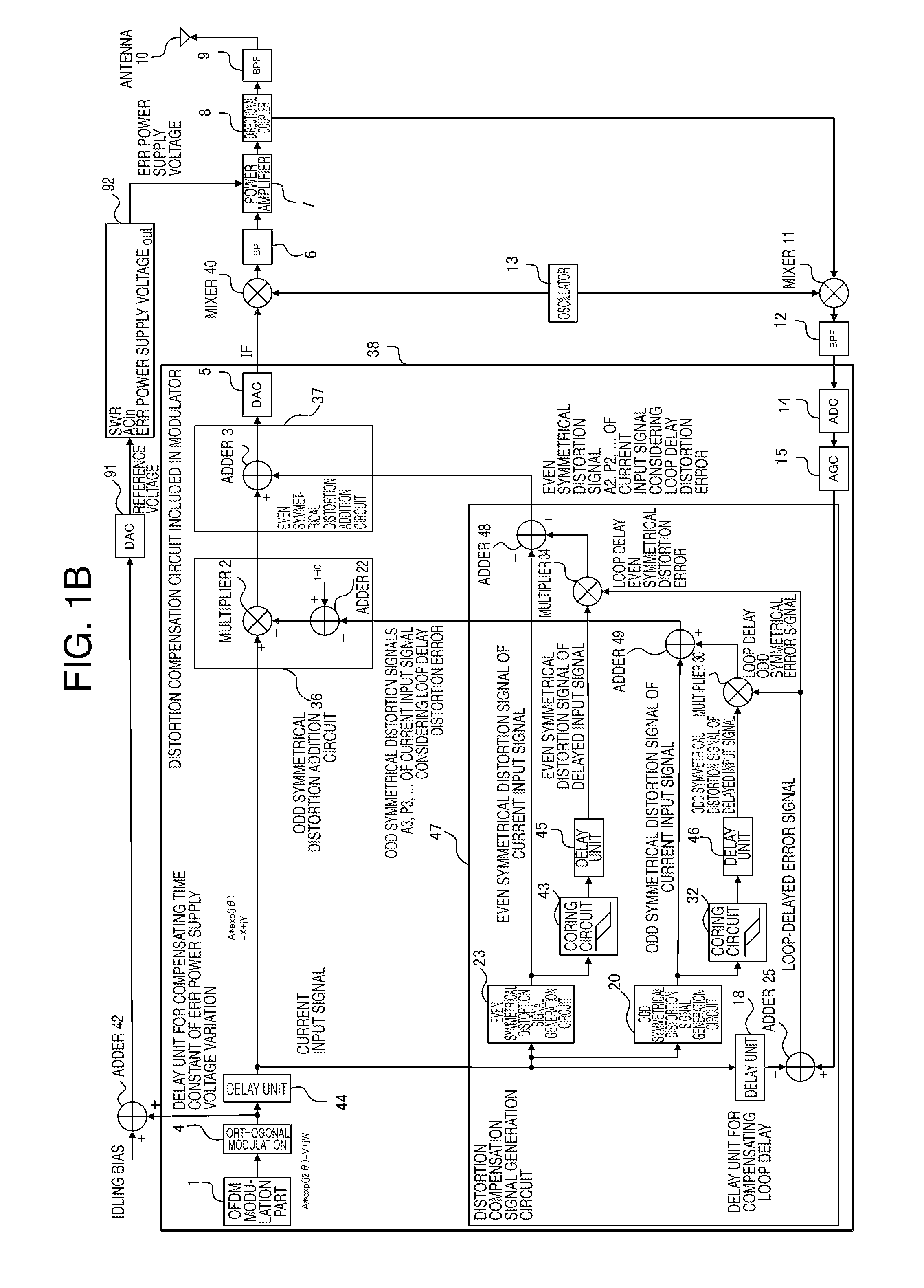
[0070]In FIG. 1B, a digital input signal produced by an OFDM modulator 1 provided in a distortion compensation circuit 38 included in a modulator of the present invention is modulated by an orthogonal modulator (orthogonal modulation) 4 ...


PUM


Abstract

The purpose of the invention is to reduce Cartesian loop transmission delay for compensating the distortion occurring in a high-frequency power amplifier and make the distortion compensation converge quickly, thereby increasing the efficiency. A transmission device has: a high-frequency power amplifier; a pre-distortion compensation circuit for independently generating the coefficients of the distortion compensation signal for each order of the odd and even symmetric distortions of the high-frequency power amplifier; a means for varying the power supply voltage of the high-frequency power amplifier with an orthogonal modulation OFDM input signal; a digital frequency converter; a high-frequency band ADC; and a high-frequency band DAC. In the transmission device, an error distortion compensation signal is created from the output of the high-frequency power amplifier and the orthogonal modulation OFDM input signal, and a delay device is inserted at the previous stage of a distortion compensation circuit, said delay device having a delay equivalent to a time constant for varying the power supply voltage of the high-frequency power amplifier with the orthogonal modulation OFDM input signal.

Description

TECHNICAL FIELD[0001]The present invention relates to distortion compensation to reduce a distortion component produced by a transmission device which transmits radio waves which are power-amplified by a high-frequency power amplifier.BACKGROUND ART[0002]The orthogonal frequency division multiplexing (OFDM) modulation method (hereinafter referred to as OFDM method) and the quardrature amplitude modulation method (hereinafter referred to as QAM method) are adopted in the terrestrial digital broadcasting and the multimedia broadcasting. The modulation signal in the terrestrial digital broadcasting and the multimedia broadcasting is constructed by constituent unit periods and has average power and peak power of a signal which are considerably different.[0003]When the linearity is ensured by supplying a power amplifier with such a fixed voltage as to be able to produce peak power in a power amplification system, the time that the peak power is produced is extremely short and as a result...

Claims


Application Information

Patent Timeline
Patent Type & Authority Applications(United States)
IPC IPC(8): H03F1/32H03F3/19H03F3/21
CPCH03F1/3241H03F3/21H03F2200/171H03F2201/3209H03F2201/3227H03F3/19H03F1/32H03F3/24H03F1/0211H04L27/2614H04L27/367H04B1/0475H04B2001/0425H03F1/0227
Inventor HIROSE, NOBUONAKAMURA, KAZUHIKO
Owner KOKUSA ELECTRIC CO LTD
Why Eureka
Try Eureka