Quasi-nanowire transistor and method of manufacturing the same

a nanowire transistor and nanowire technology, applied in the field of semiconductor technology, can solve the problems of deterioration of the electrical properties of the device, increase in power consumption, and decrease of the signal-to-noise ratio (snr), and achieve the effect of effective control of the gate length characteristics, reducing the short channel effect of the device, and improving the performance of the semiconductor devi

Inactive Publication Date: 2015-09-10
INST OF MICROELECTRONICS CHINESE ACAD OF SCI
View PDF9 Cites 11 Cited by
  • Summary
  • Abstract
  • Description
  • Claims
  • Application Information

AI Technical Summary

Benefits of technology

[0023]In the quasi-nanowire transistor and a method of manufacturing the same provided by the present invention, source/drain regions are firstly formed and then a quasi-nanowire fin is formed, which can control gate length characteristics effectively, e.g., gate length and the alignment of the bottom and the top. In addition, the high-k gate dielectric and the metal gate ca

Problems solved by technology

Short channel effect leads to the deterioration of the electrical properties of the device, e.g., leading to problems such as reduction of the gate threshold voltage, increase in power consumption, and signal-to-noise ratio (SNR) decline.
However, the manufacture of a fully depleted device requires the thickness of the silicon layer in the channel to be quite small.
Traditional manufacturing processes, especially traditional bulk silicon-based processes can hardly ma

Method used


Image

  • Quasi-nanowire transistor and method of manufacturing the same
  • Quasi-nanowire transistor and method of manufacturing the same
  • Quasi-nanowire transistor and method of manufacturing the same

Examples


Embodiment Construction

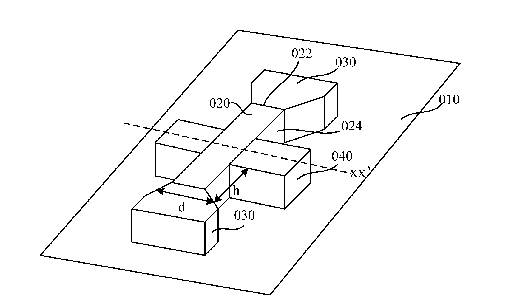
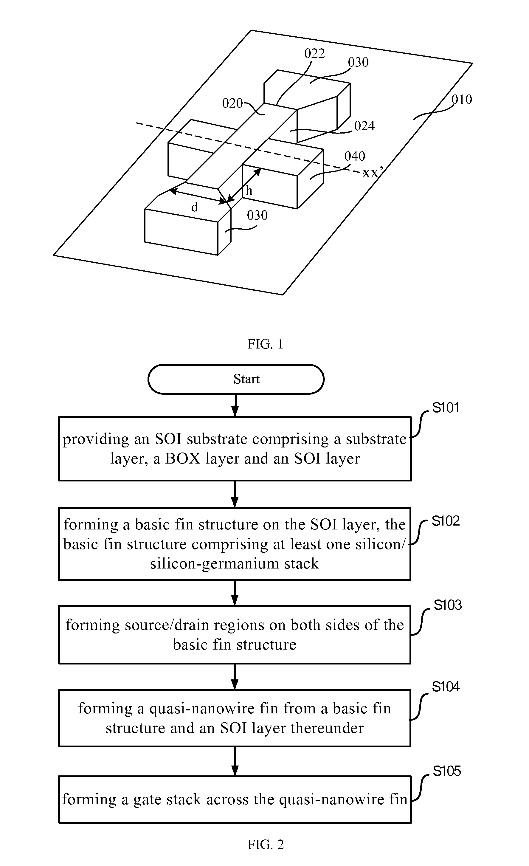
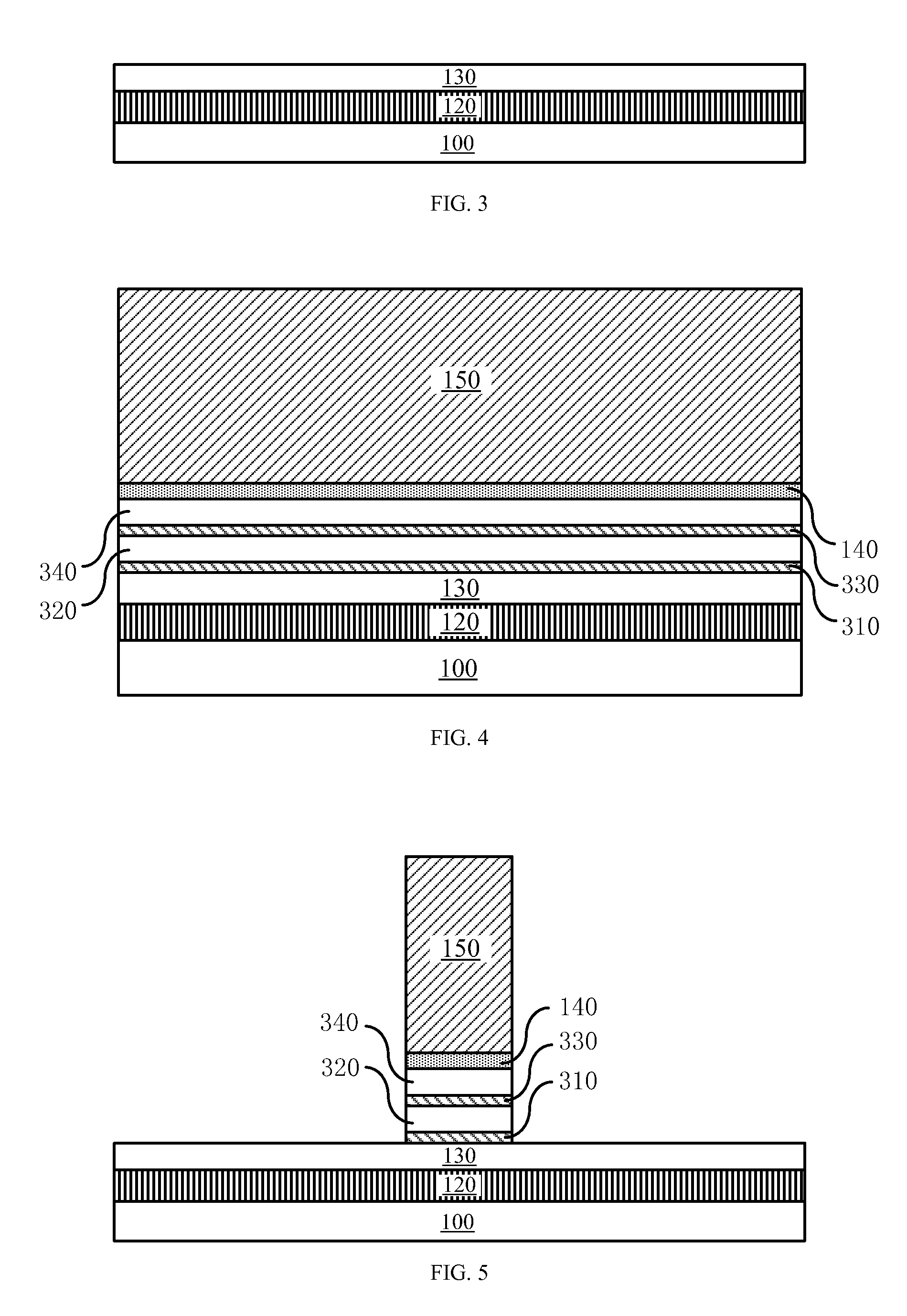
[0044]To make the objects, technical solutions and advantages of the present invention more clear, the embodiments of the present invention will be described in detail with reference to the drawings.

[0045]The embodiments of the present invention are described below in detail and the illustrative examples of the embodiments are shown in the drawings, wherein the same or similar reference numbers denote the same or similar elements or components having the same or similar functions throughout the drawings. The embodiments described with reference to drawings are exemplary, which are used for explaining the present invention only, and cannot be construed as limiting the present invention.

[0046]The following disclosure provides many different embodiments or examples used to achieve different structures of the present invention. In order to simplify the disclosure of the present invention, members of examples and arrangements thereof will be described hereinafter. Of course, they are mer...


PUM


Abstract

A quasi-nanowire transistor and a method of manufacturing the same are provided, the quasi-nanowire transistor comprising: providing an SOI substrate comprising a substrate layer (100), a BOX layer (120) and an SOI layer (130); forming a basic fin structure on the SOI layer, the basic fin structure comprising at least one silicon/silicon-germanium stack; forming source/drain regions (110) on both sides of the basic fin structure; forming a quasi-nanowire fin from a basic fin structure and an SOI layer thereunder; and forming a gate stack across the quasi-nanowire fin. The method can effectively control gate length characteristics. A semiconductor structure formed by the above method is also provided.

Description

[0001]This application claims the benefits of prior Chinese Patent Application No. 201210407807.8 filed on Oct. 23, 2012, titled “QUASI-NANOWIRE TRANSISTOR AND METHOD OF MANUFACTURING THE SAME”, which is incorporated herein by reference in its entirety.TECHNICAL FIELD[0002]The present invention relates to the field of semiconductor technology. In particular, the present invention relates to a quasi-nanowire transistor and a method of manufacturing the same.BACKGROUND ART[0003]As the channel length of Metal Oxide Semiconductor Field Effect Transistors (MOSFETs) continues to scale, a series of effects that can be neglected in the long-channel model of MOSFETs become more significant, and even become the dominant factor that affects the performance. Such phenomenon is generally referred to as short channel effect. Short channel effect leads to the deterioration of the electrical properties of the device, e.g., leading to problems such as reduction of the gate threshold voltage, increas...

Claims


Application Information

Patent Timeline
IPC IPC(8): H01L29/78H01L27/12H01L29/66
CPCH01L29/785H01L27/1203H01L29/66795H01L29/7848H01L29/0673H01L29/1054H01L29/16H01L29/66439H01L29/775H01L29/78696
Inventor ZHU, HUILONGLIANG, QINGQINGYIN, HAIZHOULUO, ZHIJIONG
Owner INST OF MICROELECTRONICS CHINESE ACAD OF SCI
Why Eureka
Try Eureka