Nanofiber and photovoltaic device comprising patterned nanofiber

a nanofiber and photovoltaic technology, applied in the field of nanofibers, can solve the problems of not exploring the effect of the fiber architecture on the opv performance, the quantum efficiency of opv is relatively limited, and the application of such nanofibers in bulk-heterojunction opv devices has not been explored, so as to improve the charge drift velocity, enhance the exciton generation of p3ht, and reduce the electrical resistance

Active Publication Date: 2015-09-17
NAT TAIWAN UNIV
View PDF6 Cites 1 Cited by
  • Summary
  • Abstract
  • Description
  • Claims
  • Application Information

AI Technical Summary

Benefits of technology

[0018]According to the embodiments of the present invention, incorporating the nanofibers of the present invention into P3HT:PCBM OPV improves the charge drift velocity and further reduces the electrical resistance, particularly for the composite nanofibers with fused joints (i.e. non-woven and crossed-patterns). Additi

Problems solved by technology

However, with the comparatively low charge carrier mobility (usually less than 10−4 cm2V−1s−1) of photo-active polymers, the quantum efficiency of OPV is relatively limited.
Therefore, it remains a challenge using thin polymer films to create a more efficient light trapping and

Method used


Image

  • Nanofiber and photovoltaic device comprising patterned nanofiber
  • Nanofiber and photovoltaic device comprising patterned nanofiber
  • Nanofiber and photovoltaic device comprising patterned nanofiber

Examples


example 1

Preparation of the Ag / PVP Composite Nanofibers (AgF-1)

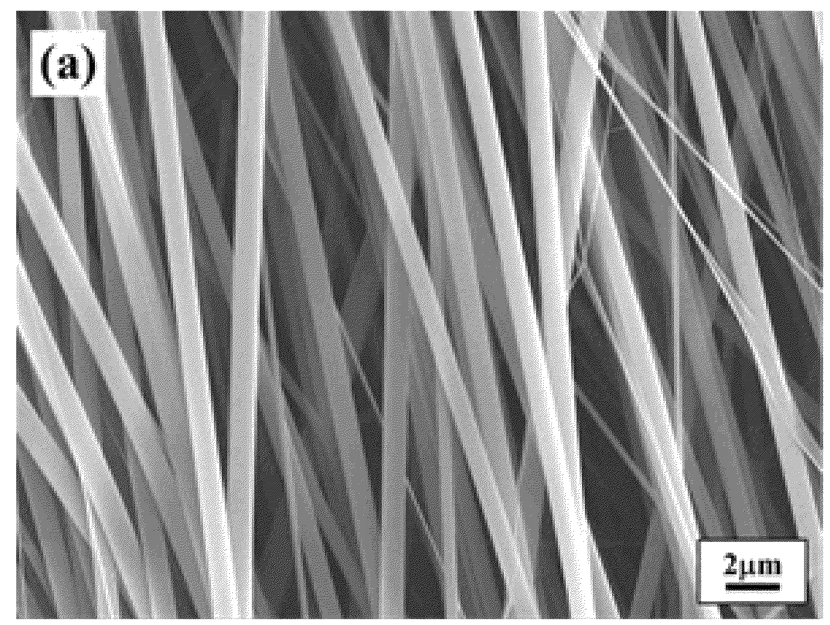
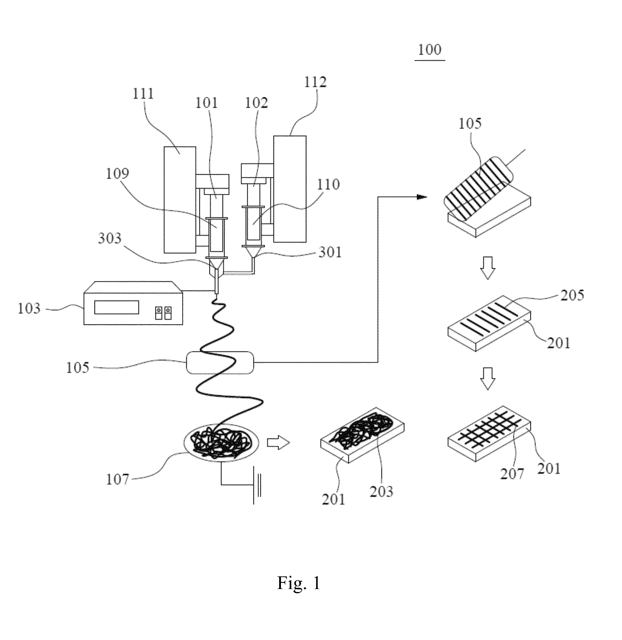
[0038]FIG. 1 illustrates the coaxial Electrospinning (ES) devices and its use of manufacturing for non-woven, aligned, or crossed-pattern nanofiber layer. As FIG. 1 showed, the nanofiber and the photovoltaic devices containing the same can be prepared using the preparation procedures described in the following. Using two-fluid coaxial electrospinning technique, grounded modified collector 107 was employed to produce aligned core / shell nanofibers. Specifically, two syringes 101, 102 containing core and shell solutions 303, 301 respectively were connected to separate needles 109, 110, and the needle 109 was placed one inside the other to form a two-fluid coaxial ES system 100. The core and shell solutions 303, 301 were fed into the coaxial capillaries by two syringe pumps 111, 112 (KD Scientific Model 100, USA).

[0039]30 mg Silver oxide (Ag2O, ≧99.99% trace metals basis) were added into ammonium hydroxide solution (ACS reagent, 28.0...

example 2

Preparation of the Ag / PVP Composite Nanofibers (AgF-2)

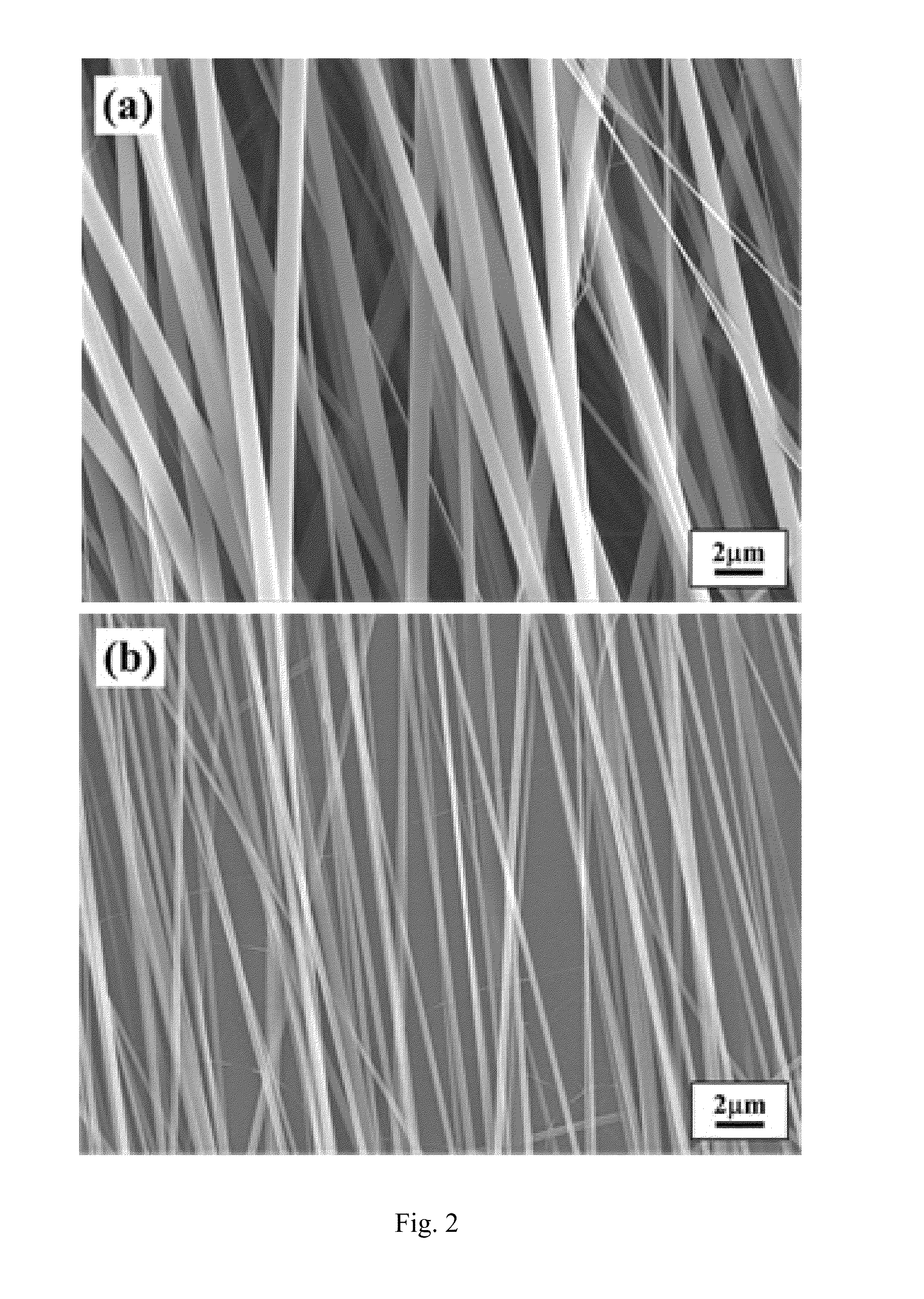
[0044]The example was prepared using the same preparation procedures as Example 1, except that 30 mg Ag2O was replaced by 5 mg Ag2O to add into 1 ml ammonium hydroxide solution to form Ag(NH3)2+ complex ion as the core solution 303 of AgF-2. 100 mg mL−1 of PVP dissolved in methanol as shell solution 301 of AgF-2 with 30 wt % of TBAP was added to increase conductivity and then stabilize the cone-jet. The same method as Example 1 was used to characterize the morphology and electrical property of the nanofibers.

example 3

Preparation of the Ag / PVP Composite Nanofibers (AgF-3)

[0045]The example was prepared using the same preparation procedures as Example 1, except that 30 mg Ag2O was replaced by 1 mg Ag2O to add into 1 ml ammonium hydroxide solution to form Ag(NH3)2+ complex ion as the core solution 303 of AgF-3. 100 mg mL−1 of PVP dissolved in methanol as shell solution 301 in AgF-3 with 30 wt % of TBAP added to increase conductivity and then stabilize the cone-jet. The same method as Example 1 was used to characterize the morphology and electrical property of the nanofibers.


PUM

PropertyMeasurementUnit
Diameteraaaaaaaaaa
Diameteraaaaaaaaaa

Abstract

This invention provides a nanofiber, including: a core, which extends along the axis of the nanofiber, and its main component includes Ag(NH3)2+ or AgNO3; a shell, which extends along the nanofiber and coats the core of the nanofiber, and its main component of the shell structure includes: PVP, TBAP, SDS, grapheme, PMAA or PFBT nanoparticle. Moreover, the invention also provides a photovoltaic device which comprises the patterned nanofibers.

Description

BACKGROUND OF THE INVENTION[0001]1. Field of the Invention[0002]The present invention relates to a nanofiber, especially to a nanofiber and a photovoltaic device comprising patterned nanofiber.[0003]2. Description of the Related Art[0004]Large-area solution processible organic photovoltaic (OPV) have attracted extensive scientific interest for renewable energy conversion due to the advantages of inexpensive, low fabrication temperature, and mechanical flexibility. Currently, the power conversion efficiency (PCE) of polymer-fullerene bulk-heterojunction OPVs over 9-10% are reported for single junction devices as well as tandem solar cells. However, with the comparatively low charge carrier mobility (usually less than 10−4 cm2V−1s−1) of photo-active polymers, the quantum efficiency of OPV is relatively limited. Thus, it is common to use a thinner polymer film for preventing the exciton recombination, leading to higher internal quantum efficiency. The minimized photo-active layer, howe...

Claims


Application Information

Patent Timeline
IPC IPC(8): H01L51/44H01L51/00H01L51/42
CPCH01L51/447H01L51/4253H01L51/0047H01L51/0035H01L51/0036H01L51/442Y02E10/549Y02E10/52H10K30/53H10K85/113H10K85/1135H10K85/215H10K30/30H10K30/82H10K2102/103H01L31/054H10K30/20
Inventor CHEN, WEN-CHANGCHIU, YU-CHENGCHEN, JUNG-YAO
Owner NAT TAIWAN UNIV
Why Eureka
Try Eureka