
Quantum-Size-Controlled Photoelectrochemical Etching of Semiconductor Nanostructures

a photoelectrochemical and quantum-size control technology, applied in the manufacture of nanostructures, semiconductor lasers, microstructure devices, etc., can solve the problems of essentially zero etch rate and light absorption drop, so as to improve the etch rate of iii-nitride materials, reduce the volume of the film, and reduce the light absorption

Active Publication Date: 2015-09-24
NAT TECH & ENG SOLUTIONS OF SANDIA LLC
View PDF3 Cites 7 Cited by
  • Summary
  • Abstract
  • Description
  • Claims
  • Application Information

AI Technical Summary

Benefits of technology

The invention is based on a new method called QSC-PEC etching, which can be used to create semiconductor nanostructures on surfaces and in thin films. This method uses quantum-size effects in a self-consistent and self-limited manner, resulting in increased etch rates of III-nitride materials. The etching results in a nanostructured surface, with nanoparticles approaching the quantum size limit, which leads to a decrease in light absorption. The etch rate drops to almost zero due to the self-limiting etch mechanism. Overall, QSC-PEC etching offers a novel way to fabricate semiconductor nanostructures with controlled size and surface quality.

Problems solved by technology

Because the decrease of the particle size results in the decrease of light absorption, due to the decreased volume of the film for light absorption and to the increase of the bandgaps of the resulting nanoparticles due to quantum confinement effects, the etch rate drops to essentially zero due to the self-limiting etch mechanism.

Method used


Image

  • Quantum-Size-Controlled Photoelectrochemical Etching of Semiconductor Nanostructures
  • Quantum-Size-Controlled Photoelectrochemical Etching of Semiconductor Nanostructures
  • Quantum-Size-Controlled Photoelectrochemical Etching of Semiconductor Nanostructures

Examples


Embodiment Construction

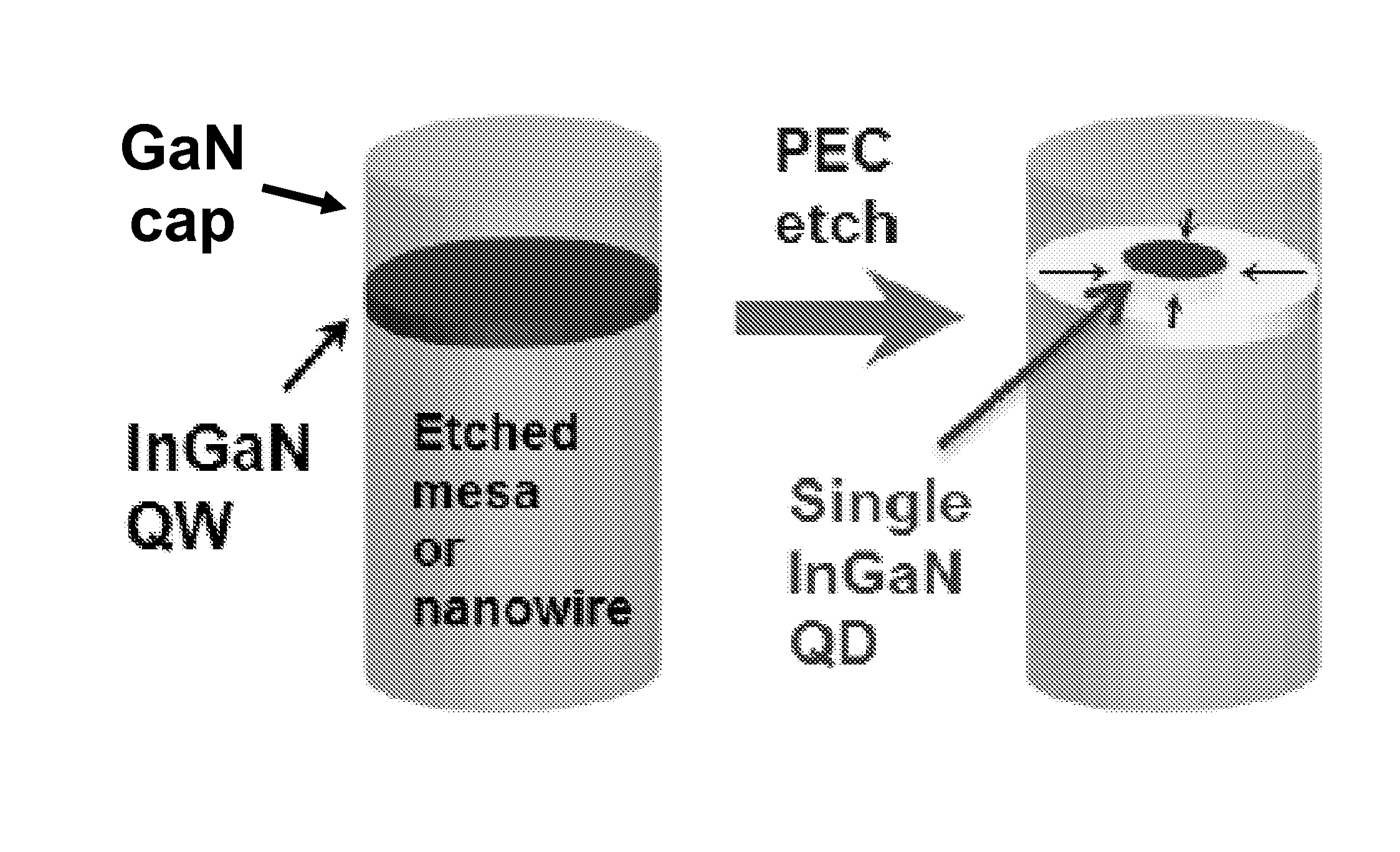
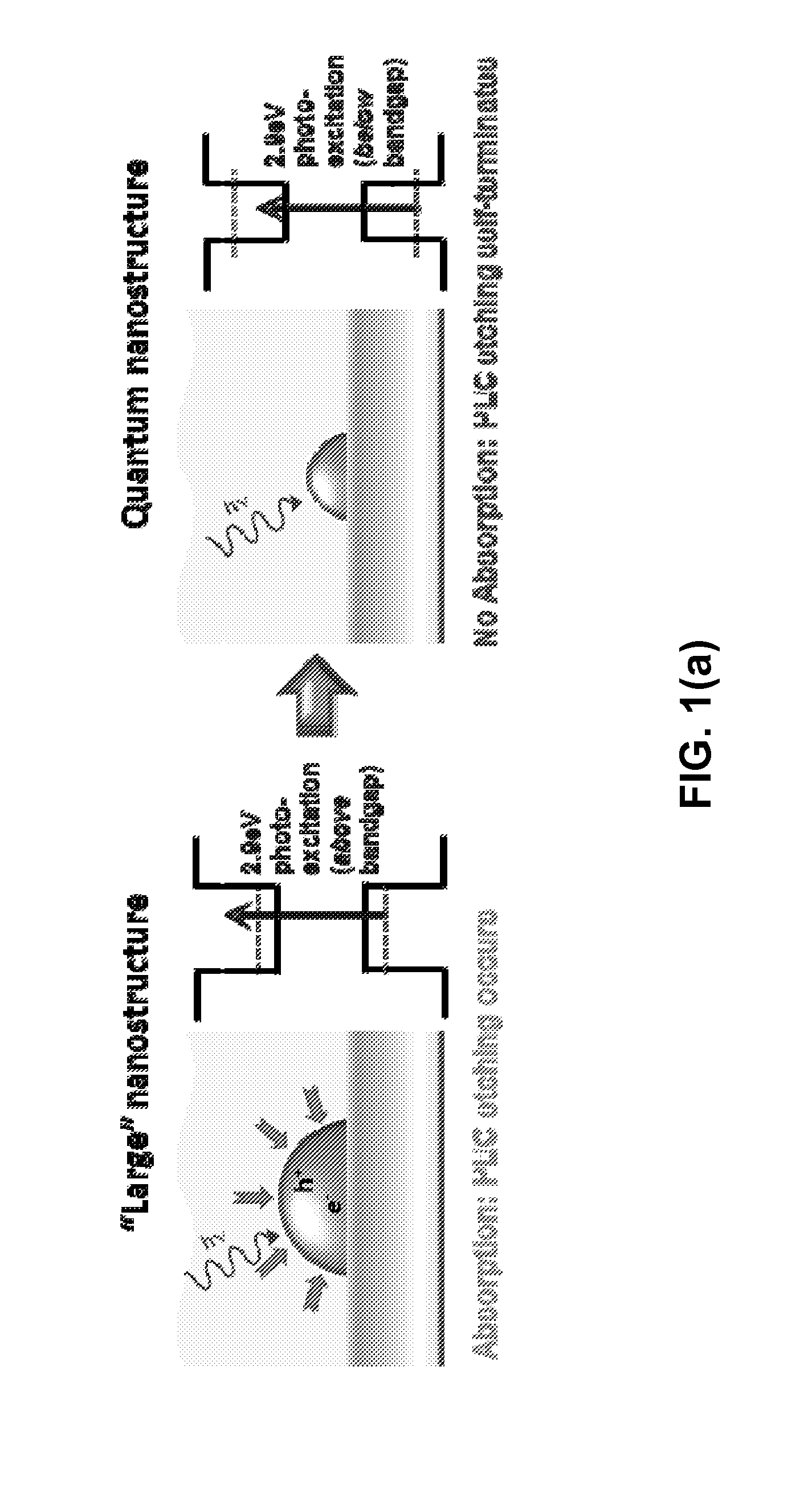
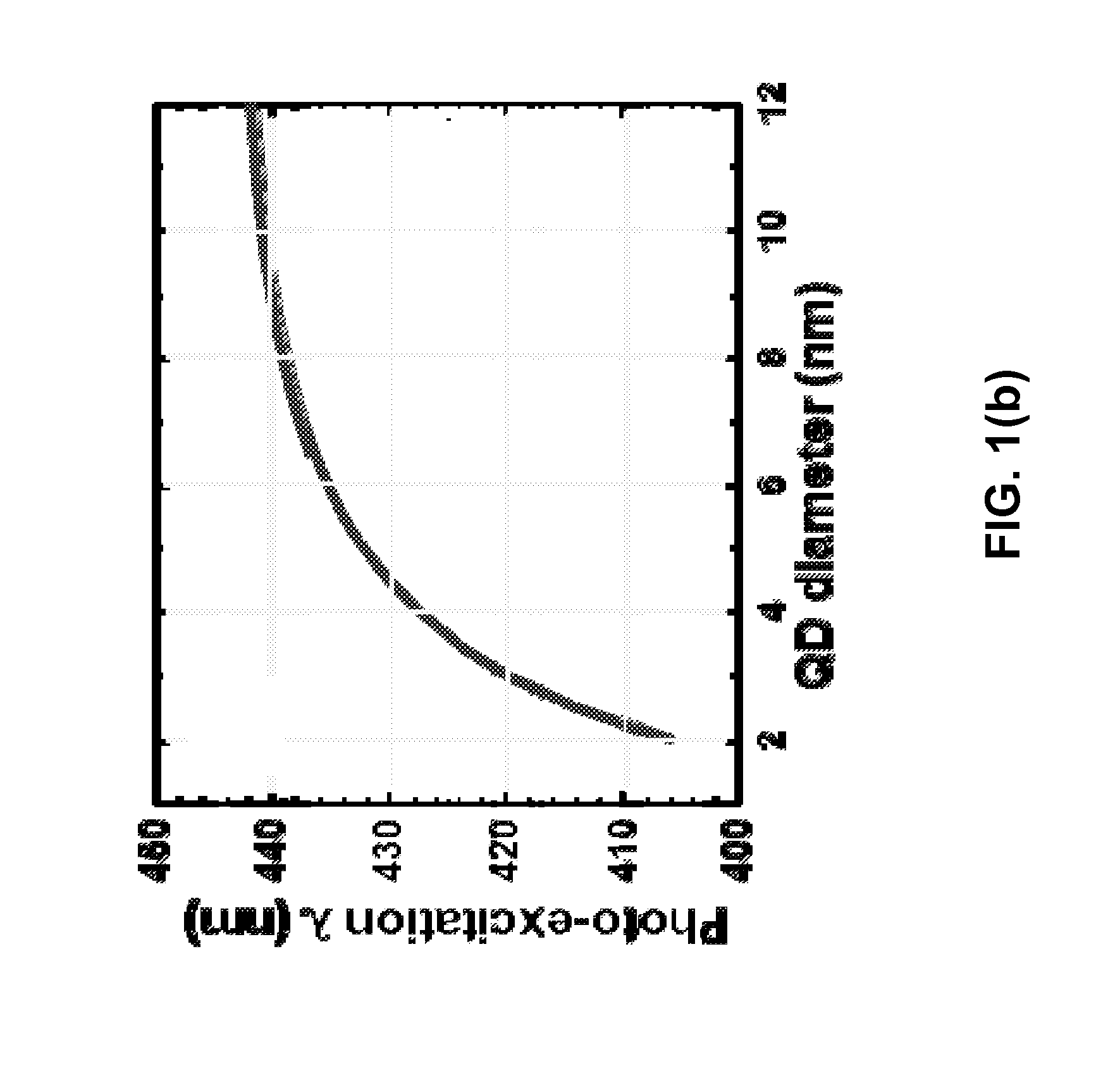
[0026]According to the present invention, quantum-size effects are used to control the fabrication of semiconductor nanostructures, with significant implications for the realization of a broad range of future nanoelectronic and nanophotonic devices. The quantum-size-controlled photoelectrochemical (QSC-PEC) etching scheme is illustrated in FIG. 1(a). The initial step in QSC-PEC etching is semiconductor surface oxidization by photoexcited holes. See A. J. Bard, Science 207, 139 (1980); and P. A. Kohl, IBM J. Res. Dev. 42, 629 (1998). Photoexcitation depends on light absorption; light absorption depends on bandgap; and in the quantum-size regime bandgap depends on nanostructure size. In particular, as the size of a nanostructure gets smaller, the bandgap goes up. Thus, properly selected narrowband light will be absorbed by large but not small nanostructures, and, therefore, PEC etching can be self-terminated at a size determined by the wavelength of that narrowband light. Although qua...


PUM


Abstract

Quantum-size-controlled photoelectrochemical (QSC-PEC) etching provides a new route to the precision fabrication of epitaxial semiconductor nanostructures in the sub-10-nm size regime. For example, quantum dots (QDs) can be QSC-PEC-etched from epitaxial InGaN thin films using narrowband laser photoexcitation, and the QD sizes (and hence bandgaps and photoluminescence wavelengths) are determined by the photoexcitation wavelength.

Description

CROSS-REFERENCE TO RELATED APPLICATION[0001]This application claims the benefit of U.S. Provisional Application No. 61 / 955,909, filed Mar. 20, 2014, which is incorporated herein by reference.STATEMENT OF GOVERNMENT INTEREST[0002]This invention was made with Government support under contract no. DE-AC04-94AL85000 awarded by the U. S. Department of Energy to Sandia Corporation. The Government has certain rights in the invention.FIELD OF THE INVENTION[0003]The present invention relates to the fabrication of semiconductor nanostructures and, in particular, to a method for quantum-size-controlled photoelectrochemical etching of semiconductor nanostructures.BACKGROUND OF THE INVENTION[0004]The past two decades have seen an explosion of interest in semiconductor nanophotonics and nanoelectronics, a large fraction enabled by controlled fabrication of epitaxial semiconductor nanostructures. See S. Kako et al., Nature Mater. 5, 887 (2006); K. J. Vahala, Nature 424, 839 (2003); and C. Weisbuch...

Claims


Application Information

Patent Timeline
IPC IPC(8): H01L21/306H01S5/343H01L33/06H01L21/3065H01L33/00
CPCH01L21/30612H01L21/3065H01S5/34333H01L33/0075H01L33/06H01L33/0062H01L33/007H01L33/18C25F3/12H01L21/30635B81C1/00539B81C2201/0114B82B1/00
Inventor FISCHER, ARTHUR J.TSAO, JEFFREY Y.WIERER, JR., JONATHAN J.XIAO, XIAOYINWANG, GEORGE T.
Owner NAT TECH & ENG SOLUTIONS OF SANDIA LLC
Learn More