Method of manufacturing light emitting device
a technology of light emitting device and manufacturing method, which is applied in the manufacture of semiconductor/solid-state devices, semiconductor devices, semiconductor devices, etc., can solve the problems of deterioration of light guide components, low thermal conductivity of light guide components made of adhesives, and difficulty in bonding sapphire substrates to light emitting elements, etc., to achieve uniform chromaticity distribution, prevent damage to luminescent color conversion members, and effectively dissipate heat generated by luminescent color conversion
- Summary
- Abstract
- Description
- Claims
- Application Information
AI Technical Summary
Benefits of technology
Problems solved by technology
Method used
Image

Examples
first embodiment
[0067]A manufacturing method of a light emitting device 10 according to a first embodiment will be described with reference to FIG. 1A to FIG. 3.
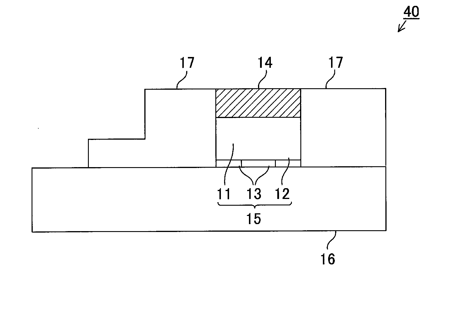
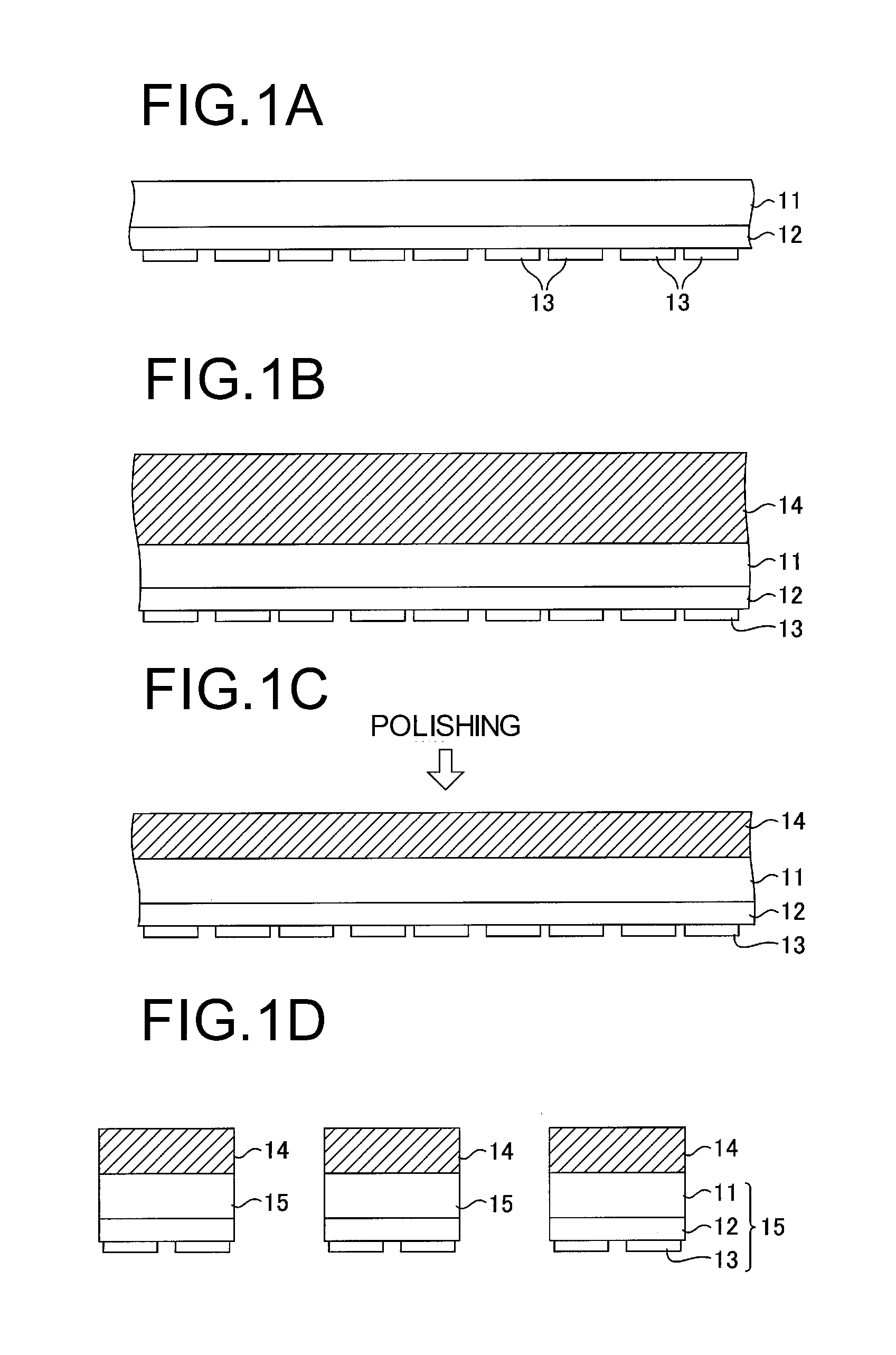
[0068]Process 1 (see FIG. 1A): A semiconductor layer (semiconductor lamination portion) 12 constituting a light emitting device structure is formed on the entire surface on a rear side of a plate-like crystal growth substrate (mounting substrate) 11. A plurality of electrodes 13 is formed on the semiconductor layer 12. Fine irregularities (not shown) for scattering the emitted light are formed on the entire surface on a front surface side (light emitting surface side) of the crystal growth substrate 11.
[0069]Meanwhile, the electrodes 13 constitute an anode-side electrode and a cathode-side electrode of an LED (Light Emitting Diode) chip 15 (to be described later).
[0070]The crystal growth substrate 11 is made of, for example, a gallium nitride substrate, a sapphire substrate, a silicon carbide substrate and the like.
[0071]Further, in order t...
second embodiment
[0111]A manufacturing method of a light emitting device 20 of a second embodiment will be described with reference to FIG. 1, FIG. 4 and FIG. 5.
[0112]Process 1 (see FIG. 1A), Process 2 (see FIG. 1B) and Process 3 (see FIG. 10): Same as Process 1 to Process 3 of the first embodiment.
[0113]Process 4 (see FIG. 4A): Without using an adhesive, the light scattering member 21 having a flat surface is directly fixed to the entire surface on the front side of the luminescent color conversion member 14.
[0114]The light scattering member 21 is formed by a translucent material (e.g., a sintered body of a glass, a thermoplastic resin material, a thermosetting resin material, and a transparent inorganic material such as a sol-gel glass and alumina, etc.). The translucent material contains a light scattering material (e.g., silica, titanium oxide, etc.) for scattering the emitted light of the LED chip 15.
[0115]Meanwhile, the light scattering member 21 may be formed by the translucent material in wh...
third embodiment
[0132]A manufacturing method of a light emitting device 30 of a third embodiment will be described with reference to FIGS. 1A to 1D, FIG. 2A and FIGS. 6A to 6B.
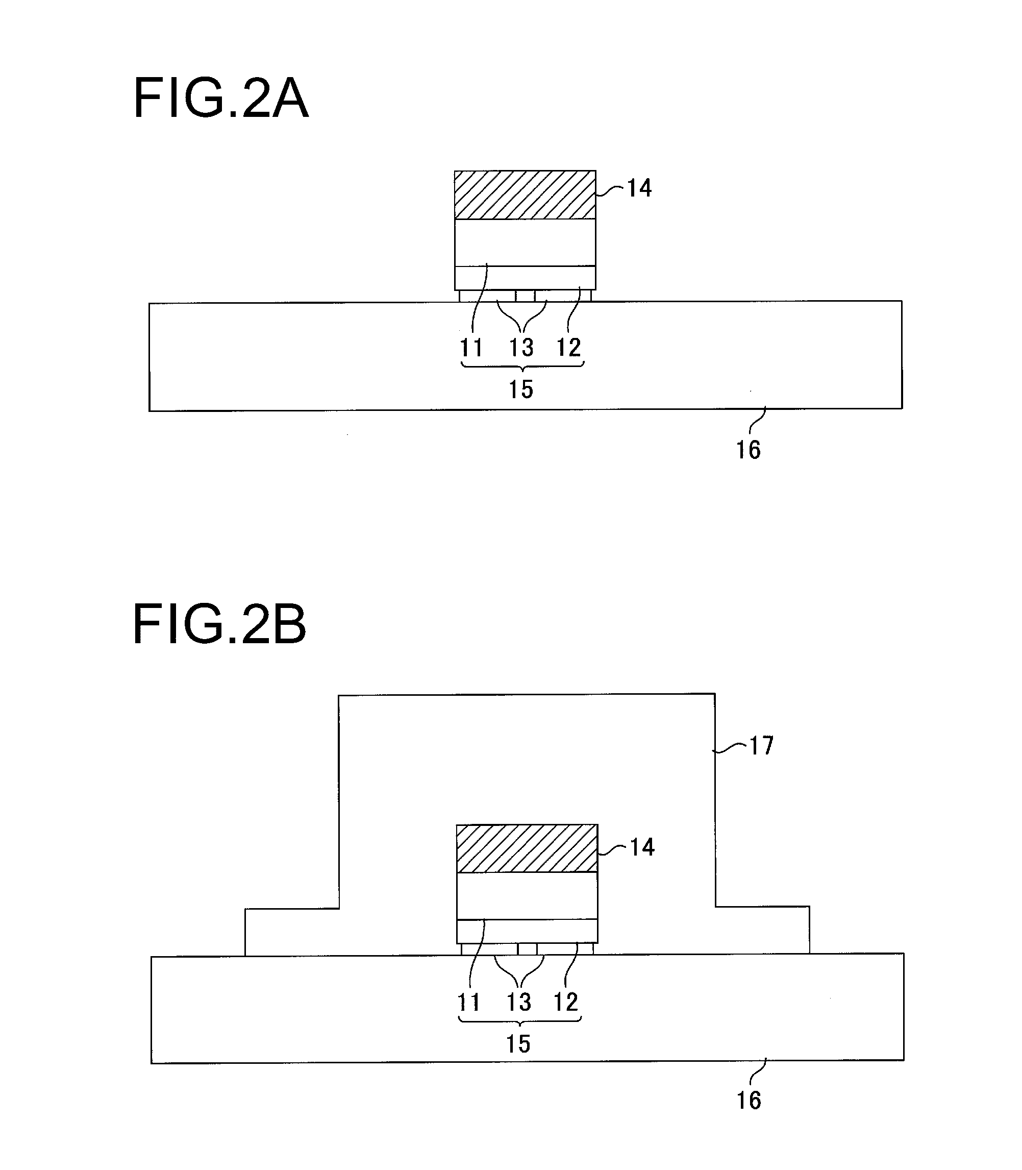
[0133]Process 1 (see FIG. 1A), Process 2 (see FIG. 1B), Process 3 (see FIG. 10), Process 4 (see FIG. 10) and Process 5 (see FIG. 2A): Same as Process 1 to Process 5 of the first embodiment.
[0134]Process 6 (see FIG. 6A): A reflective member 31 is formed on the front surface of the mounting substrate 16.
[0135]The reflective member 31 has a double layer structure where a light reflective layer 31a and a light absorption layer 31b are laminated. The reflective member 31 has an insulating property.
[0136]The light reflective layer 31a surrounds the luminescent color conversion member 14 and the LED chip 15 and is in close contact with the side surfaces thereof.
[0137]The light absorption layer 31b surrounds the luminescent color conversion member 14. The light absorption layer 31b is in close contact with the vicinity of the upper e...
PUM
 Abstract
Description
Claims
Application Information
 - R&D
- Intellectual Property
- Life Sciences
- Materials
- Tech Scout
- Unparalleled Data Quality
- Higher Quality Content
- 60% Fewer Hallucinations
Browse by: Latest US Patents, China's latest patents, Technical Efficacy Thesaurus, Application Domain, Technology Topic, Popular Technical Reports.
© 2025 PatSnap. All rights reserved.Legal|Privacy policy|Modern Slavery Act Transparency Statement|Sitemap|About US| Contact US: help@patsnap.com