Semiconductor device, electronic component, and electronic device

a technology of semiconductor devices and components, applied in semiconductor devices, digital storage, instruments, etc., can solve problems such as data loss, and achieve the effect of increasing layout area and speed

Inactive Publication Date: 2015-10-15
SEMICON ENERGY LAB CO LTD
View PDF7 Cites 15 Cited by
  • Summary
  • Abstract
  • Description
  • Claims
  • Application Information

AI Technical Summary

Benefits of technology

[0010]Another object of one embodiment of the present invention is to provide a semiconductor device or the like having a novel structure which can include more components without an increase in layout area. Another object of one embodiment of the present invention is to provide a semiconductor device or the like having a novel structure which can operate at higher speed.
[0017]Alternatively, according to one embodiment of the present invention, a semiconductor device or the like having a novel structure which can include more components without an increase in layout area can be provided. Consequently, a smaller semiconductor device or the like having a novel structure can be provided according to one embodiment of the present invention. Alternatively, according to one embodiment of the present invention, a semiconductor device or the like having a novel structure which can operate at higher speed can be provided.

Problems solved by technology

Since SRAMs are volatile memories, data is lost when power supply is stopped.

Method used


Image

  • Semiconductor device, electronic component, and electronic device
  • Semiconductor device, electronic component, and electronic device
  • Semiconductor device, electronic component, and electronic device

Examples


embodiment 1

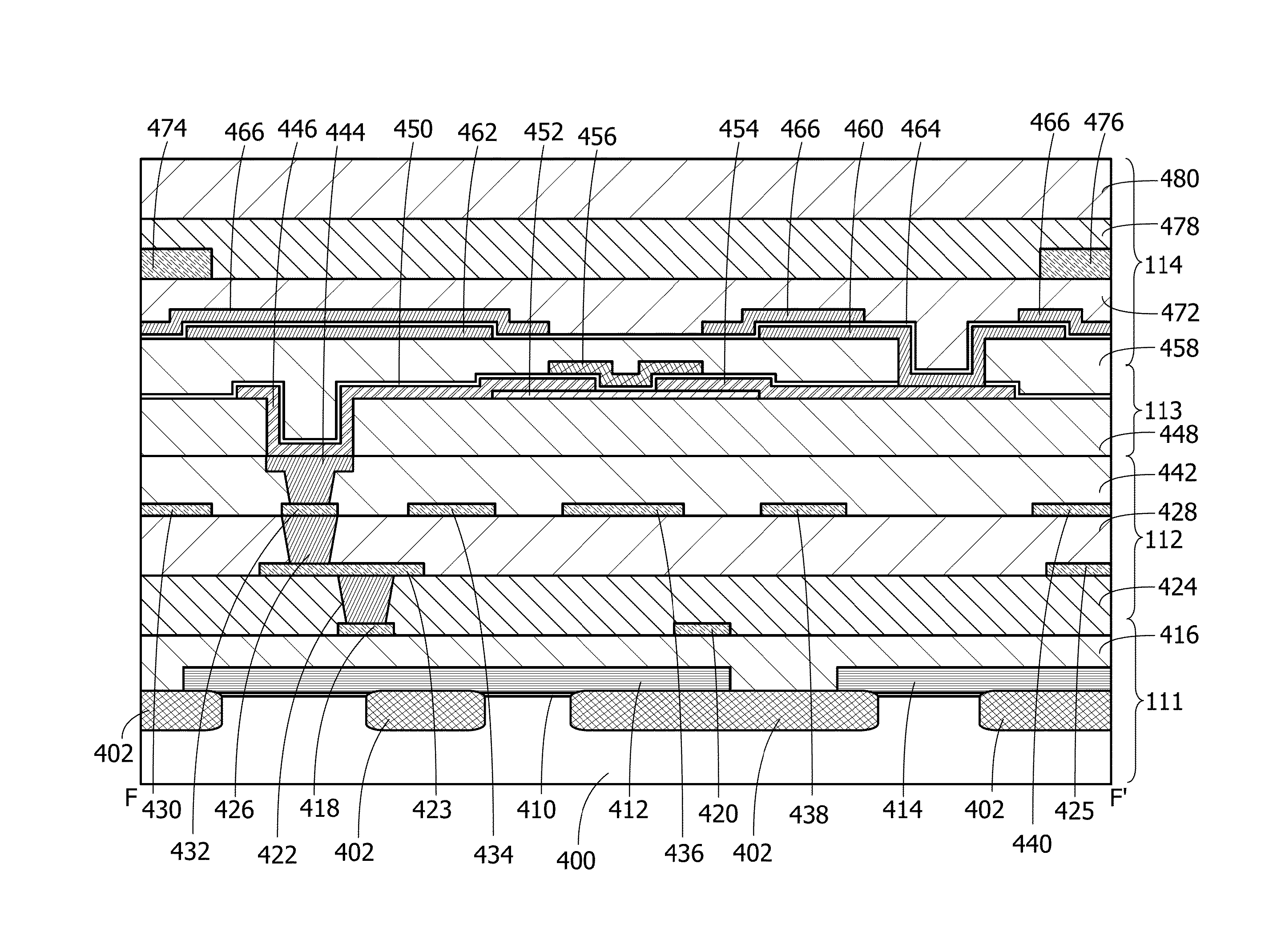
[0058]In this embodiment, circuit diagrams, top views, cross-sectional views, and a timing chart of a semiconductor device are described.

[0059]In this specification and the like, a semiconductor device means all devices that can function by utilizing semiconductor characteristics. The term “semiconductor device” refers to a memory such as a cache formed using semiconductor elements, e.g., transistors, peripheral circuits for controlling the memory, a CPU which inputs / outputs a signal to / from the memory and the peripheral circuits, a power supply voltage supplying circuit, a power management unit, and the entire system including the circuits.

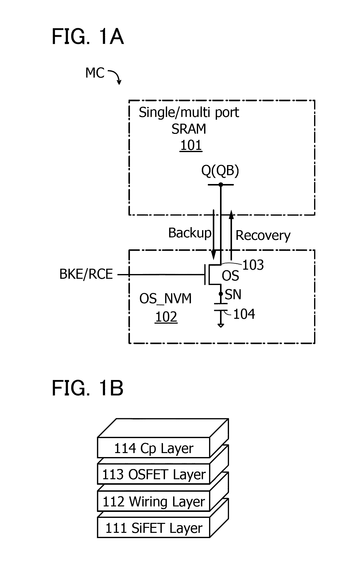
[0060]As one embodiment of the semiconductor device, a configuration of a memory cell MC is described.

[0061]FIG. 1A is an outline circuit diagram of the memory cell MC.

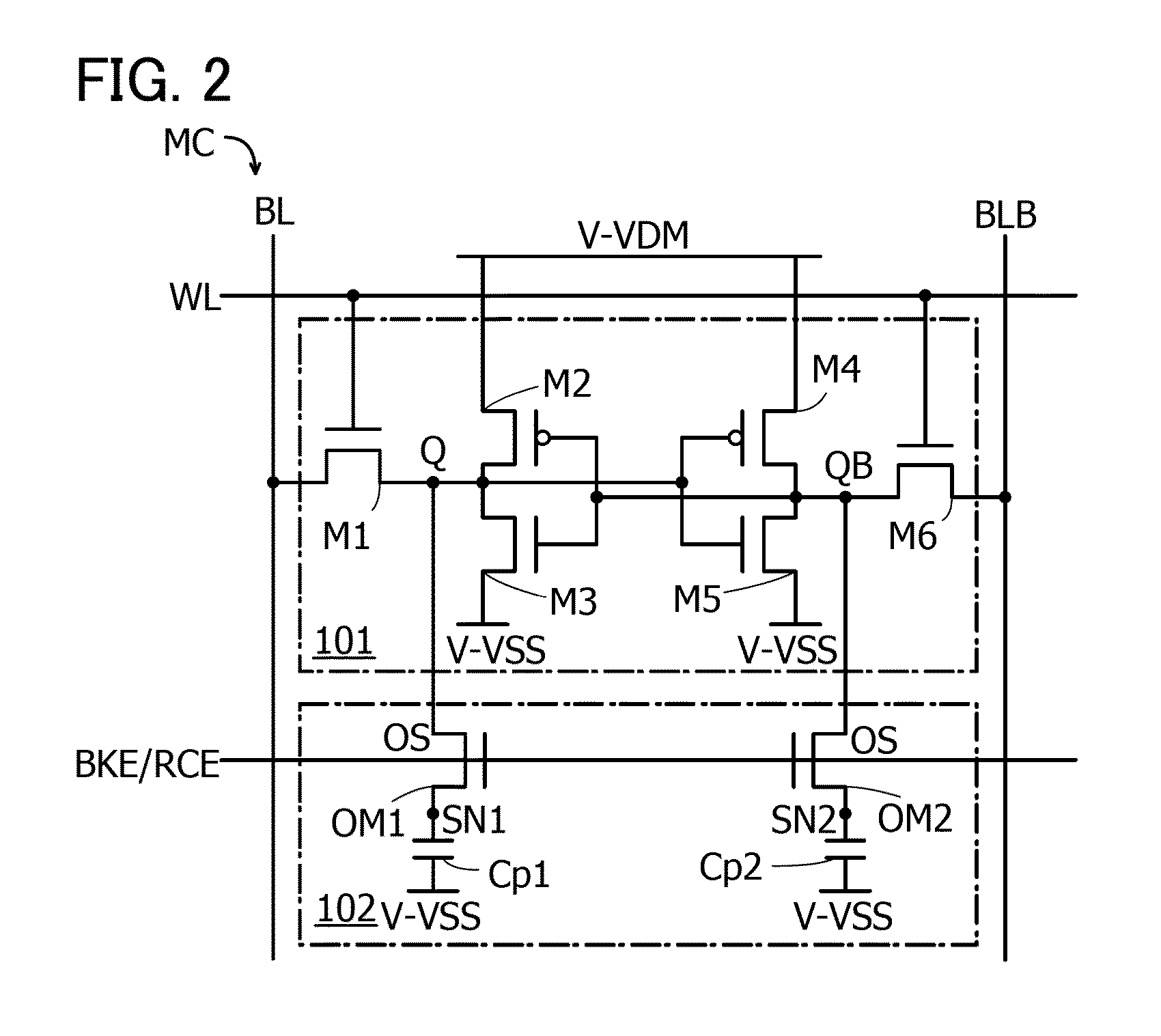
[0062]The memory cell MC illustrated in FIG. 1A includes an SRAM101 and a data memory portion 102. The data memory portion 102 includes a transistor 103 and a capacitor 104.

[0063]T...

embodiment 2

[0151]In this embodiment, an example of the operation different from that of the memory cell MC described in the above embodiment is described.

[0152]In this embodiment, operation of the memory cell MC illustrated in FIG. 12 is described. The memory cell MC illustrated in FIG. 12 includes the multiport SRAM 101 in FIG. 7A and the data memory portion 102 in FIG. 11B for static data recovery.

[0153]Note that in FIG. 12, nodes holding charge corresponding to data in the data memory portion 102 are denoted by SN3 and SN4.

[0154]Note that a power supply voltage supplied to the inverters INV7 and INV8 in FIG. 12 may be the same as in the SRAM 101 as illustrated in FIG. 25A, or may be a power supply voltage (VDM2 / VSS) which is different from that in the SRAM 101 as illustrated in FIG. 25B.

[0155]FIGS. 13A and 13B and FIG. 14 are timing charts different from that of the operation of the memory cell MC illustrated in FIG. 12. FIGS. 13A and 13B illustrate operation of the power supply potential l...

embodiment 3

[0169]In this embodiment, configurations of block diagrams of a cache including the memory cell MC illustrated in FIGS. 1A and 1B and circuits accessing the cache are described.

[0170]A semiconductor device 30 includes a cache 300 (denoted by Cache), a power supply voltage supplying circuit 330 (denoted by Supply Voltage), a power management unit 340 (denoted by PMU), a CPU 350, an input / output interface 360 (denoted by I / O UF), and a bus interface 370 (denoted by Bus UF), as shown in FIG. 16.

[0171]The power management unit 340 has a function of performing power gating of the circuits included in the cache 300. The power management unit 340 outputs a power gating control signal (PGCS). Thus, the power consumption of the semiconductor device 30 can be reduced.

[0172]The power management unit 340 performs power gating in accordance with a sleeping signal (denoted by Sleeping) from the CPU 350, a signal from external hardware through the input / output interface 360, or a state of the bus ...


PUM


Abstract

A semiconductor device having a novel structure. A multiport SRAM and a data memory portion including an OS transistor are stacked. Since the multiport SRAM includes more wirings and transistors, an area increase is not caused by an increase in the number of transistors in the data memory portion including an OS transistor. An increase in the number of transistors in the data memory portion enables static operation. Thus, the data memory portion can achieve stable recovery operation, higher speed operation, and simplification.

Description

BACKGROUND OF THE INVENTION[0001]1. Field of the Invention[0002]One embodiment of the present invention relates to a semiconductor device, an electronic component, or an electronic device.[0003]Note that one embodiment of the present invention is not limited to the above technical field. The technical field of the invention disclosed in this specification and the like relates to an object, a method, or a manufacturing method. In addition, one embodiment of the present invention relates to a process, a machine, manufacture, or a composition of matter. Specifically, examples of the technical field of one embodiment of the present invention disclosed in this specification include a semiconductor device, a display device, a light-emitting device, a power storage device, a memory device, a method of driving any of them, and a method of manufacturing any of them.[0004]2. Description of the Related Art[0005]Static random access memories (SRAMs) are used as cache memories of processors or t...

Claims


Application Information

Patent Timeline
Patent Type & Authority Applications(United States)
IPC IPC(8): H01L27/12H01L29/24G11C14/00
CPCH01L27/1207H01L29/24G11C14/0054G11C8/16H01L27/1225
Inventor ISHIZU, TAKAHIKO
Owner SEMICON ENERGY LAB CO LTD
Why Eureka
Try Eureka