Semiconductor Device And Manufacturing Method Thereof
- Summary
- Abstract
- Description
- Claims
- Application Information
AI Technical Summary
Benefits of technology
Problems solved by technology
Method used
Image

Examples
first embodiment
A. First Embodiment
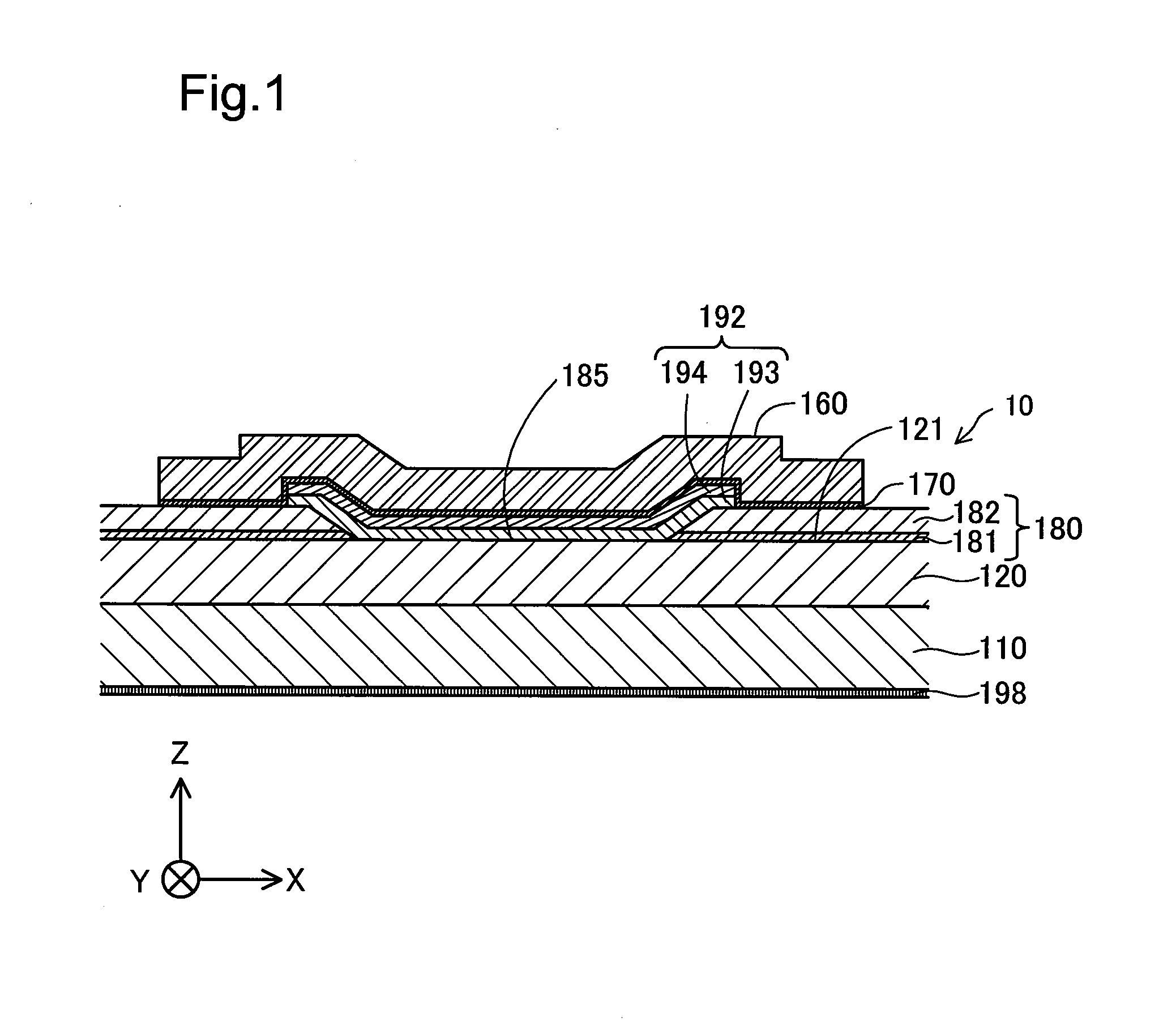
[0045]A-1. Structure of Semiconductor Device
[0046]FIG. 1 is a cross sectional view schematically illustrating the structure of a semiconductor device 10 according to a first embodiment. XYZ axes orthogonal to one another are illustrated in FIG. 1.
[0047]Among the XYZ axes in FIG. 1, the X axis is an axis going from the left side of the sheet surface to the right side of the sheet surface of FIG. 1; +X-axis direction is a direction going rightward on the sheet surface and −X-axis direction is a direction going leftward on the sheet surface. Among the XYZ axes in FIG. 1, the Y axis is an axis going from the front side of the sheet surface to the back side of the sheet surface of FIG. 1; +Y-axis direction is a direction going backward on the sheet surface and −Y-axis direction is a direction going forward on the sheet surface. Among the XYZ axes in FIG. 1, the Z axis is an axis going from the lower side of the sheet surface to the upper side of the sheet surface of FI...
second embodiment
B. Second Embodiment
[0094]FIG. 11 is a cross sectional view schematically illustrating the structure of a semiconductor device 20 according to a second embodiment. The semiconductor device 20 of the second embodiment differs from the semiconductor device 10 of the first embodiment by a Schottky electrode, a barrier metal layer and a wiring layer but otherwise has the similar structure to that of the semiconductor device 10 of the first embodiment.
[0095]According to this embodiment, a Schottky electrode 292 is made of nickel and has a film thickness of 100 nm. A barrier metal layer 270 is formed on the schottky electrode 292, is made of molybdenum and has a film thickness of 100 nm.
[0096]According to this embodiment, a wiring layer 260 is made of an aluminum silicon copper (AlSiCu) prepared by adding 0.5% of silicon (Si) and 0.5% of copper (Cu) to aluminum (Al) and has a film thickness of 4 μm. The invention may also be applicable to the semiconductor device of this structure.
third embodiment
C. Third Embodiment
[0097]FIG. 12 is a cross sectional view schematically illustrating the structure of a semiconductor device 30 according to a third embodiment. The semiconductor device 30 of the third embodiment differs from the semiconductor device 20 of the second embodiment by a barrier metal layer, a Schottky electrode and a wiring layer but otherwise has the similar structure to that of the semiconductor device 20 of the second embodiment. In the semiconductor device 30, a Schottky electrode 293 and a barrier metal layer 370 are provided only on a Schottky electrode 292, and a wiring layer 360 includes a barrier metal layer 372 on the semiconductor layer 120-side.
[0098]According to this embodiment, the wiring layer 360 is made of aluminum silicon (AlSi) prepared by adding 1% of silicon (Si) to aluminum (Al) and has a film thickness of 4 μm. The barrier metal layer 372 is made of titanium nitride (TiN) and has a film thickness of 200 nm.
[0099]The barrier metal layer 370 is mad...
PUM
 Abstract
Description
Claims
Application Information
 - R&D
- Intellectual Property
- Life Sciences
- Materials
- Tech Scout
- Unparalleled Data Quality
- Higher Quality Content
- 60% Fewer Hallucinations
Browse by: Latest US Patents, China's latest patents, Technical Efficacy Thesaurus, Application Domain, Technology Topic, Popular Technical Reports.
© 2025 PatSnap. All rights reserved.Legal|Privacy policy|Modern Slavery Act Transparency Statement|Sitemap|About US| Contact US: help@patsnap.com