Photoelectric conversion device, solid-state image pickup unit, and electronic apparatus

a conversion device and solid-state image technology, applied in the direction of solid-state devices, thermoelectric devices, semiconductor devices, etc., can solve the problems of deterioration in quantum efficiency, degradation of flexibility in material selection of organic semiconductors, and easy degradation of photoelectric conversion layers, so as to reduce the variation in film quality in suppress the effect of heat treatment-induced deterioration in the performance of the photoelectric conversion layer

Active Publication Date: 2015-10-29
SONY CORP
View PDF3 Cites 25 Cited by
  • Summary
  • Abstract
  • Description
  • Claims
  • Application Information

AI Technical Summary

Benefits of technology

[0010]According to the photoelectric conversion device, the solid-state image pickup unit, and the electronic apparatus of the embodiments of the present disclosure, the photoelectric conversion layer includes the first organic semiconductor of the first conductive type and the second organic semiconductor of the second conductive type, and is configured by addition of a derivative or an isomer of one of them. Therefore, aggregation of the first or second organic semiconductor in high-temperature heat treatment of the manufacturing process is allowed to be inhibited, thereby reducing variation in film quality in the photoelectric conversion layer. Accordingly, deterioration in performance of the photoelectric conversion layer caused by heat treatment is allowed to be suppressed.

Problems solved by technology

Incidentally, since organic semiconductors are poor in heat resistance, performance of the photoelectric conversion layer is easily deteriorated by high-temperature heat treatment during a manufacturing process.
However, interposition of such an intermediate layer causes degradation in quantum efficiency, and also causes degradation in flexibility in material selection of organic semiconductors.

Method used


Image

  • Photoelectric conversion device, solid-state image pickup unit, and electronic apparatus
  • Photoelectric conversion device, solid-state image pickup unit, and electronic apparatus
  • Photoelectric conversion device, solid-state image pickup unit, and electronic apparatus

Examples


embodiment

Configuration

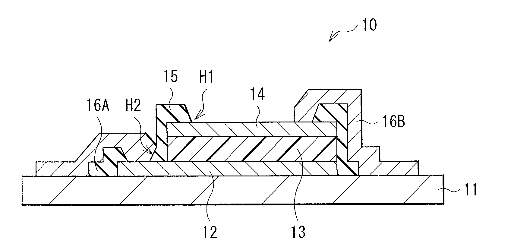
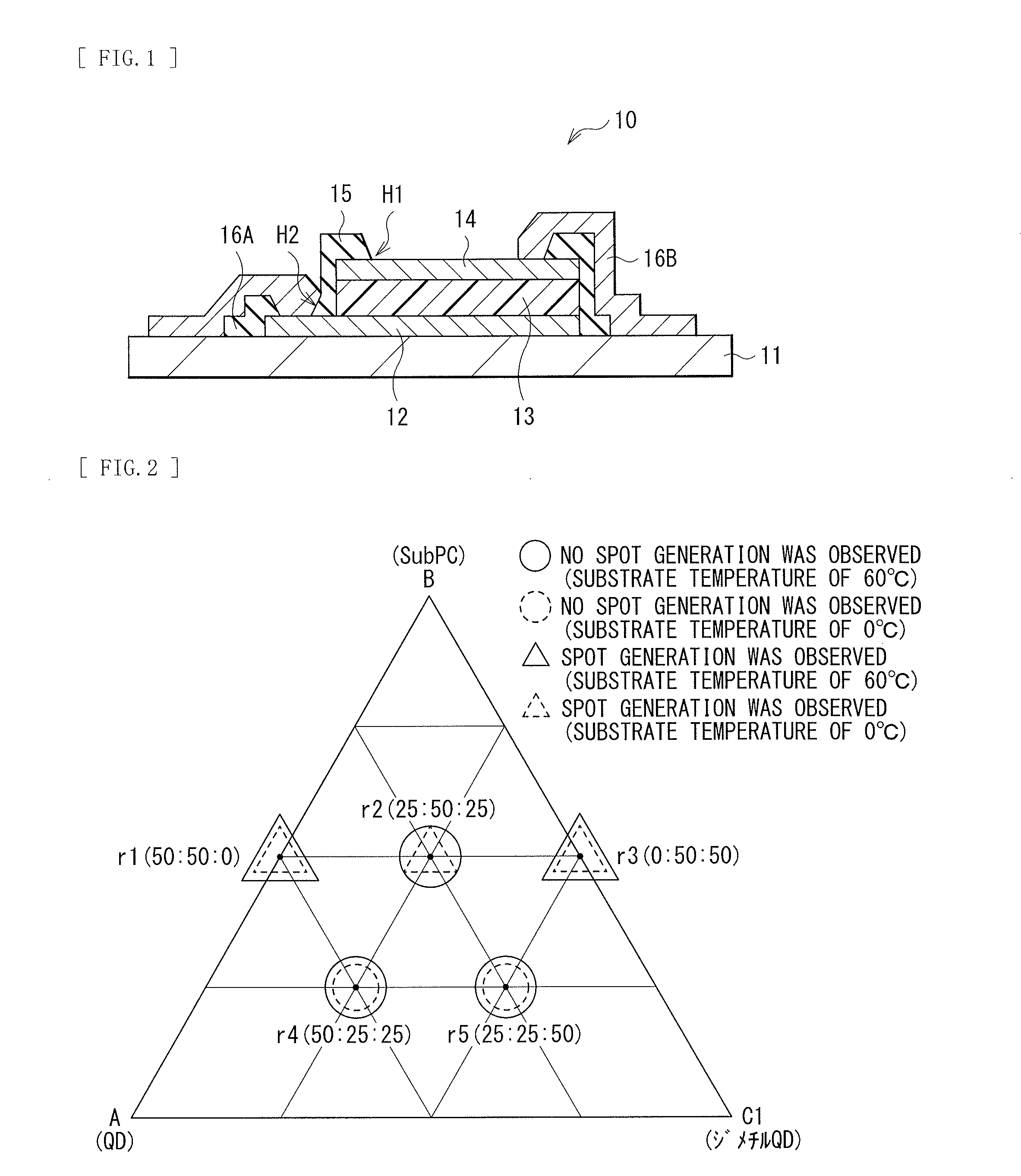
[0026]FIG. 1 illustrates a schematic sectional configuration of a pixel (a photoelectric conversion device 10) in a solid-state image pickup unit according to an embodiment of the present disclosure. As will be described in detail later, the solid-state image pickup unit may be, for example, a CCD (Charge Coupled Device) or CMOS (Complementary Metal Oxide Semiconductor) image sensor or the like. The photoelectric conversion device 10 may be provided on, for example, a substrate 11 including a pixel transistor and a wiring line, and may be coated with a sealing film, a planarization film, and the like that are not illustrated. For example, an on-chip lens that is not illustrated may be provided on the planarization film.

[0027]The photoelectric conversion device 10 is an organic photoelectric conversion device that absorbs light of a selective wavelength (for example, color light of any one of R, G, and B) with use of an organic semiconductor to generate an electron-hole ...

modification example

[0050]FIG. 11 illustrates an example of a ternary system mixture ratio of organic semiconductors (organic semiconductors A, B, and C2) included in the organic layer 13 according to the modification example. In this modification example, the organic layer 13 includes the organic semiconductor A (quinacridone) and the organic semiconductor B (subphthalocyanine) that are similar to those in the above-described embodiment, and the organic semiconductor C2 (dichloroquinacridone) different from the organic semiconductor C1 is added as a derivative of the organic semiconductor A to the organic layer 13. FIG. 11 illustrates the ternary system mixture ratios (A:B:C2) of the organic semiconductors A, B, and C2=s1 (50:50:0), s2 (25:50:25), s3 (0:50:50), s4 (50:25:25), s5 (25:25:50), and s6 (50:0:50), and presence or absence of spot generation of the organic layer 13 in these respective cases. It is to be noted that, as with the above-described embodiment, this is based on results of observing ...

application example

[0058]The above-described solid-state image pickup unit 1 is applicable to all types of electronic apparatuses having an image pickup function, for example, camera systems such as digital still cameras and video cameras, and cellular phones having an image pickup function. FIG. 13 illustrates a schematic configuration of an electronic apparatus 2 (a camera) as an example. The electronic apparatus 2 may be, for example, a video camera capable of taking a still image or a moving image, and includes the solid-state image pickup unit 1, an optical system (an optical lens) 310, a shutter unit 311, a drive section 313 that drives the solid-state image pickup unit 1 and the shutter unit 311, and a signal processing section 312.

[0059]The optical system 310 is configured to guide image light (incident light) from a subject to the pixel section 1a of the solid-state image pickup unit 1. This optical system 310 may be configured of a plurality of optical lenses. The shutter unit 311 is configu...


PUM


Abstract

A solid-state image pickup unit of the invention includes a plurality of pixels, each of which includes a photoelectric conversion element. The photoelectric conversion element includes a photoelectric conversion layer; and first and second electrodes provided with the photoelectric conversion layer in between, the photoelectric conversion layer including a first organic semiconductor of a first conductive type and a second organic semiconductor of a second conductive type, and being configured by addition of a third organic semiconductor made of a derivative or an isomer of one of the first and second organic semiconductors.

Description

TECHNICAL FIELD[0001]The present disclosure relates to a photoelectric conversion device using an organic photoelectric conversion material, and a solid-state image pickup unit and an electronic apparatus that include such a photoelectric conversion device as a pixel.BACKGROUND ART[0002]As a solid-state image pickup unit such as a CCD (Charge Coupled Device) image sensor or a CMOS (Complementary Metal Oxide Semiconductor) image sensor, a solid-state image pickup unit using a photoelectric conversion layer made of an organic semiconductor for each pixel has been proposed (for example, PTL 1).CITATION LISTPatent Literature[0003]PTL 1: Japanese Unexamined Patent Application Publication No. 2011-187918SUMMARY OF INVENTION[0004]Incidentally, since organic semiconductors are poor in heat resistance, performance of the photoelectric conversion layer is easily deteriorated by high-temperature heat treatment during a manufacturing process. Therefore, in the above-described PTL 1, to prevent ...

Claims


Application Information

Patent Timeline
Patent Type & Authority Applications(United States)
IPC IPC(8): H01L51/00
CPCH01L51/0046H01L51/0072H01L27/307H01L51/4246H01L51/0068Y02E10/549H10K39/32H10K85/657H10K85/311H10K30/211H10K30/30H01L31/10H10K85/211H10K85/655H10K85/6572
Inventor UDAKA, TORUMURATA, MASAKIENOKI, OSAMUAONUMA, MASAYOSHIMIYAJI, SAEITO, TAKUYASUDOU, MIKIMORIMOTO, RUISASAKI, HIROTO
Owner SONY CORP
Why Eureka
Try Eureka