Laser device for projecting a structured light pattern onto a scene

a laser device and structured light technology, applied in semiconductor lasers, instruments, television systems, etc., can solve the problems of known optical systems suffering from loss of brightness and optical efficiency, and achieve the effects of reducing the number of spots, reducing ambiguities, and reducing the difficulty of information extraction

Active Publication Date: 2015-11-05
TRUMPF PHOTONIC COMPONENTS GMBH
View PDF4 Cites 99 Cited by
  • Summary
  • Abstract
  • Description
  • Claims
  • Application Information

AI Technical Summary

Benefits of technology

[0012]In a further embodiment of the laser device with VCSEL arrays also the shape of the emission area of the VCSELs, i. e. the emitting aperture or active region of the VCSELs, is varied. With such a variation of the VCSEL shape ambiguities in the recorded image for 3D information extraction are resolved more easily. As a consequence the number of spots can be reduced and less than 300 horizontal spots are required in the above mentioned application to fulfill the EU-NCAP safety norm. The need for a larger number of beam spots partially is based on the need to resolve ambiguities and not only for angular resolution. Using two different VCSEL shapes already reduces the ambiguities. Preferably at least three different VCSEL shapes are used, e. g. circle, horizontal rectangle and vertical rectangle. Such shapes can be distinguished by a camera observing the scene onto which the structured light pattern is projected, since the camera resolution is significantly higher than the array resolution. The different VCSEL shapes can be provided on each array, on only one of the arrays or different arrays can provide different VCSEL shapes. If

Problems solved by technology

These known optical systems suffer from a loss in brightn

Method used


Image

  • Laser device for projecting a structured light pattern onto a scene
  • Laser device for projecting a structured light pattern onto a scene
  • Laser device for projecting a structured light pattern onto a scene

Examples


Embodiment Construction

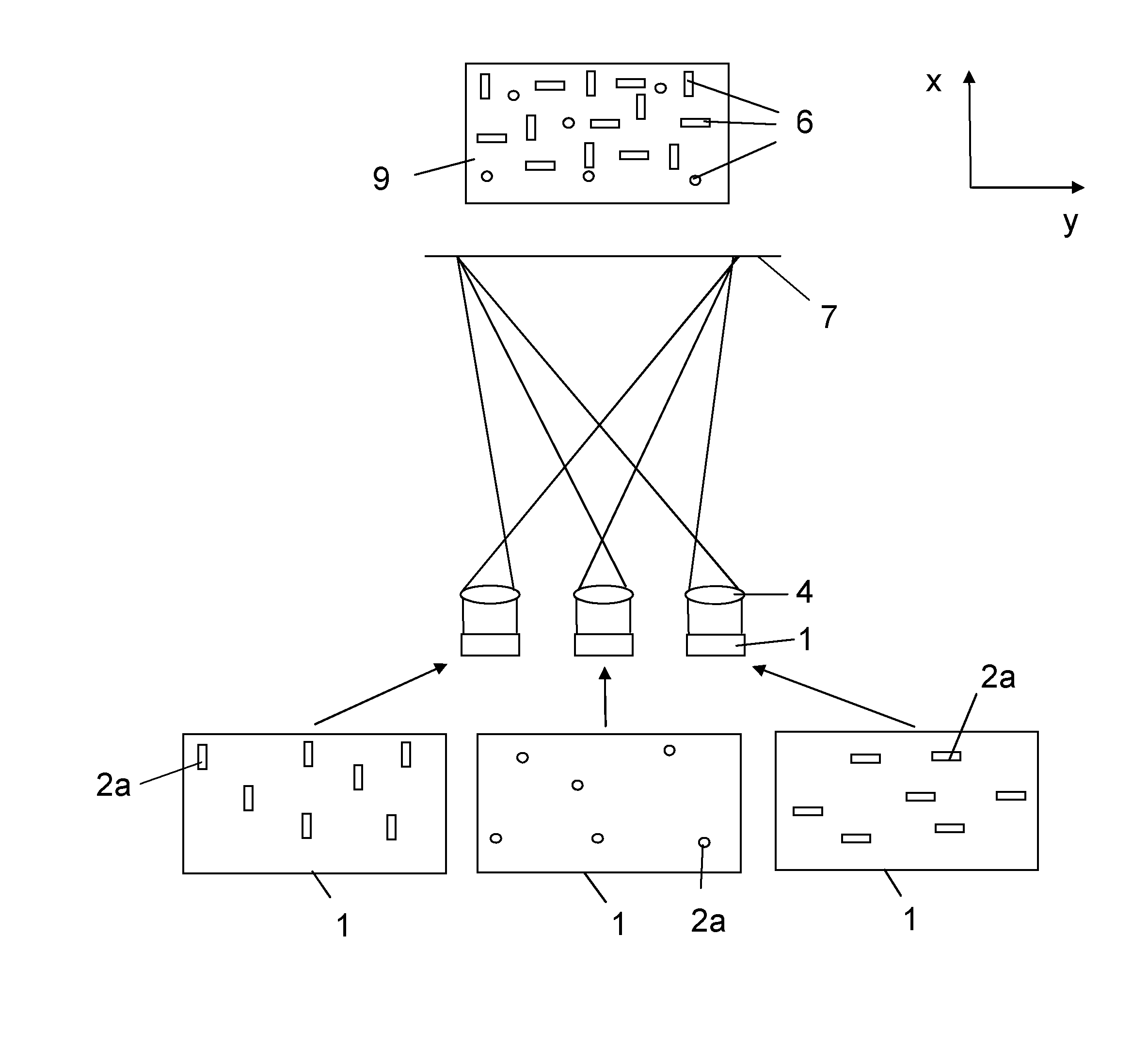
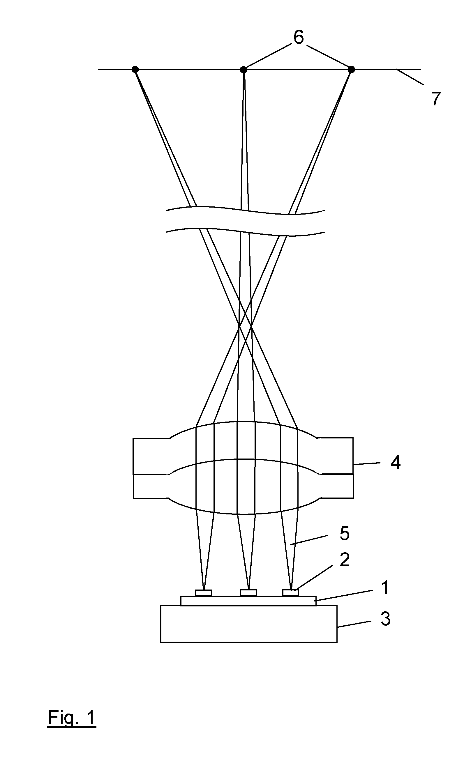
[0021]The proposed laser device comprises several semiconductor arrays with corresponding optics to image the emission areas of the semiconductor lasers to an image space. FIG. 1 shows an example for a basic layout of one module of the proposed laser device. Each module comprises one of the VCSEL-arrays used in this example. The VCSEL array is provided in a package providing electrical contacts and heat removal. FIG. 1 shows the corresponding VCSEL chip 1 carrying the VCSEL array with several VCSELs 2. The VCSEL chip 1 is mounted on a heat sink 3 for heat removal. An imaging lens 4 is arranged in front of the VCSEL-chip 1 to image the emission areas of the individual VCSELs 2 of the array to an image plane 7 in the desired image space. The image space is a depth region, also called capturing area in case of a 3D imaging system, into which the VCSEL array is imaged by the lens 4. The imaging conditions to image an e. g. a VCSEL 2 having a 4 μm diameter active area to the image space ...


PUM


Abstract

The present invention relates to a laser device (10) for projecting a structured light pattern (9) onto a scene (15). The device is formed of several arrays (1) of semiconductor lasers (2), each array (1) comprising an irregular distribution of emission areas (2a) of the semiconductor lasers (2). One or several imaging optics (4) image said arrays (1) to an imaging space and superpose the images of said arrays (1) in the imaging space to form said light pattern (9). The proposed laser device generates a light pattern with high contrast and efficiency which may be used for 3D imaging systems, e. g. in automotive applications.

Description

FIELD AND BACKGROUND OF THE INVENTION[0001]The present invention relates to a laser device for projecting a structured light pattern onto a scene using several arrays of semiconductor lasers, in particular vertical cavity surface emitting lasers (VCSELs). Structured light patterns projected onto a scene and observed with a camera enable the extraction of 3D information by image processing. Such a method is applied e. g. in the Microsoft Kinect™ game console and recently discussed for industrial applications, especially in the automotive field. In this field the new EU-NCAP safety norm enforces a distance measurement which is able to detect pedestrians and provides a resolution which allows autonomous measures taken by the car system.[0002]The required structured light pattern can be generated by dedicated micro-optical systems like micro-lens arrays or diffractive optical elements (DOE) which are illuminated by a laser, e. g. by an array of VCSELs. An example is shown in US 2012 / 051...

Claims


Application Information

Patent Timeline
IPC IPC(8): G01B11/25H04N5/265H04N5/235H01S5/42H01S5/00G01S17/89G01S17/931
CPCG01B11/254H01S5/423H04N5/265H04N5/235H01S5/005H01S5/18394G01S17/46G01S17/89G01S7/4815G01B11/2513G01S17/931H01S5/426H04N23/70
Inventor MOENCH, HOLGERGRONENBORN, STEPHANCARPAIJ, MARK
Owner TRUMPF PHOTONIC COMPONENTS GMBH
Why Eureka
Try Eureka