Device and method for analyzing defects by using heat distribution measurement

a technology of heat distribution measurement and device, applied in the direction of material thermal analysis, material flaw investigation, instruments, etc., can solve the problems of defect generation, defect reduction, defect detection, etc., and achieve high resolution and sensitivity, the effect of high accuracy

Active Publication Date: 2015-11-05
KOREA BASIC SCI INST
View PDF4 Cites 14 Cited by
  • Summary
  • Abstract
  • Description
  • Claims
  • Application Information

AI Technical Summary

Benefits of technology

[0029]According to embodiments of the present invention described above, the semiconductor manufacturing companies require the spatial resolution higher than that of the defect inspection apparatus which is currently commercialized, and thus, there is an effect that is possible to respond to their requirement.
[0030]Further, as a spectral imaging equipment is provided in the thermoreflectance microscope, the wavelength dependency of the thermoreflectance coefficient which is different according to the material and structure of the sample is measured and then the optimal wavelength is selected through the wavelength dependency. It is possible that the thermal image of the sample is achieved by the optimal wavelength with the high resolution and sensitivity. In result, the semiconductor defect position can be tracked and analyzed with high accuracy.

Problems solved by technology

Recently, due to the high integration and miniaturization of semiconductor devices, and complexity of the manufacturing process thereof, various defects that cause problems in the operations of the devices have been generated.
Such defects serve as the cause for reduction of performance and yield of the semiconductor device, and thus the semiconductor device manufacturing companies are putting a lot of efforts into addressing this problem.
In general, the defects are known to be caused by a mask misalignment, contaminants, voids, and non-uniformity of an impurity concentration inside the semiconductor devices, etc.
Many types of defects such as a metal short, resistive open, micro-plasma leakage, oxide layer breakdown, and device latch-up in the semiconductor device cause a hot spot.
However, in infrared thermal emission technique, the physical limit of spatial resolution is about 3 μm due to the optical diffraction limit, and thus, there is a limit on the accuracy of defect position tracking in the highly integrated and fine patterned semiconductor device.
However, there are still many problems in which these characteristic measurement methods have been little utilized for the defect analysis of the semiconductor device so far.
Some methods may have to cut the sample, and some methods need an excessive amount of time, etc.
When the semiconductor device is analyzed, the sample wafer may get damaged in wafer cutting process, which may cause the defect analysis impossible.
Furthermore, since various types of materials such as a metal, a dielectric, a semiconductor material, and the like are exposed on the surface of the semiconductor device, it may be difficult to effectively measure the heat distribution using the common thermoreflectance microscope.

Method used


Image

  • Device and method for analyzing defects by using heat distribution measurement
  • Device and method for analyzing defects by using heat distribution measurement
  • Device and method for analyzing defects by using heat distribution measurement

Examples


Embodiment Construction

[0035]Hereinafter, exemplary embodiments of the present invention will be described in detail with reference to the accompanying drawings. However, the present invention is not limited to the exemplary embodiments disclosed below, but can be implemented in various forms. The following exemplary embodiments are described in order to enable those of ordinary skill in the art to embody and practice the invention.

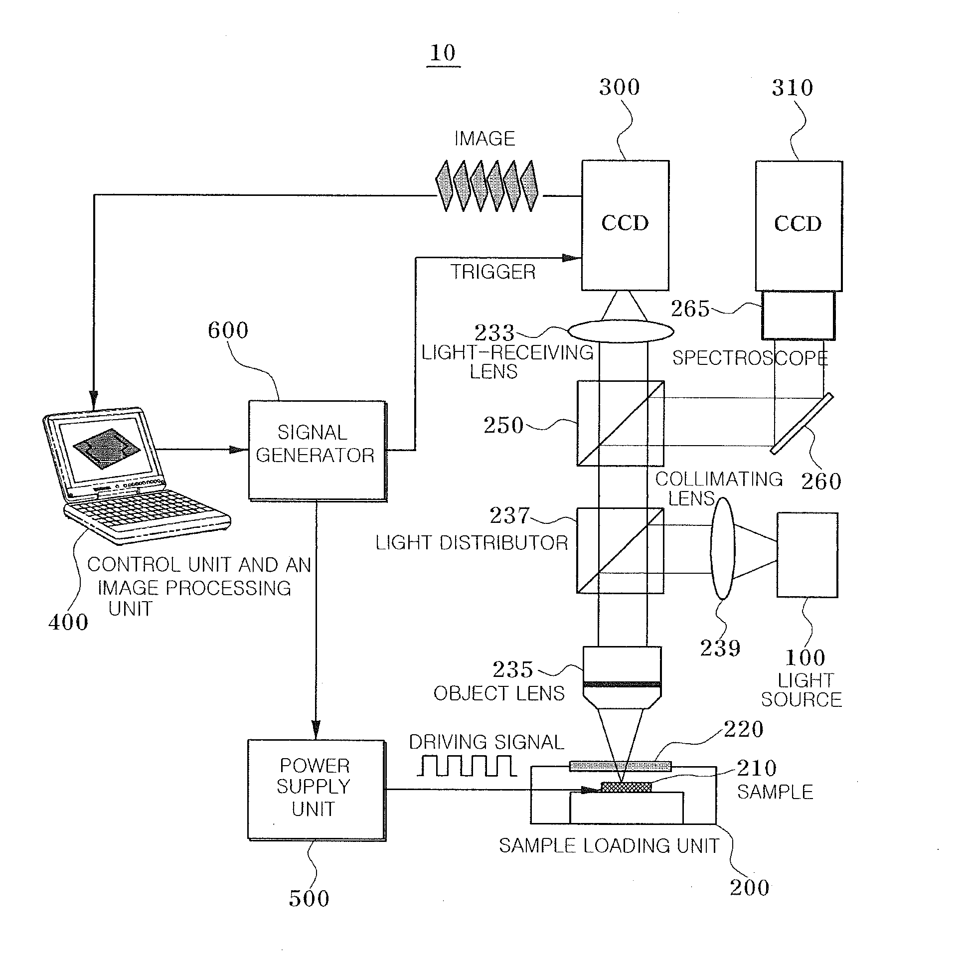
[0036]FIG. 1 is a schematic view illustrating a configuration of a defect analysis apparatus according to an embodiment of the present invention.

[0037]Referring to FIG. 1, the defect analysis apparatus according to the embodiment of the present invention includes a light source 100, a sample loading unit 200, a first detection unit 300, a control unit and an image processing unit 400, a power supply unit 500, a signal generator 600, a lock-in correlator (not shown), a first light distributor 237, and various lenses 233, 235, and 239. Meanwhile, a second beam splitter 250, a spe...


PUM

PropertyMeasurementUnit
sizesaaaaaaaaaa
wavelengthaaaaaaaaaa
specific wavelengthaaaaaaaaaa

Abstract

The present invention provides a method for analyzing defects by using heat distribution measurement, comprising: a sample loading unit for loading a sample to check whether or not there is a defect through heat distribution characteristics; a light source for radiating visible light onto the sample; a power supply unit for generating a driving signal in order to periodically heat the sample; a detection unit for detecting reflected light from the surface of the sample; and a signal generator for synchronizing the detection unit with the driving signal of the power supply unit.

Description

TECHNICAL FIELD[0001]The present invention relates to an apparatus and method for analyzing defects using heat distribution measurement, and more particularly, to an apparatus and method for analyzing defects capable of measuring hot spots caused by flaws (or defects) of a semiconductor device using a sub-micron spatial resolution and a non-contact method. The apparatus can analyze positions of the defects with high accuracy by overlapping the hot spots with a semiconductor fine pattern image.BACKGROUND ART[0002]Recently, due to the high integration and miniaturization of semiconductor devices, and complexity of the manufacturing process thereof, various defects that cause problems in the operations of the devices have been generated. Such defects serve as the cause for reduction of performance and yield of the semiconductor device, and thus the semiconductor device manufacturing companies are putting a lot of efforts into addressing this problem.[0003]In general, the defects are kn...

Claims


Application Information

Patent Timeline
Patent Type & Authority Applications(United States)
IPC IPC(8): G01N25/72
CPCG01N25/72H01L22/12H01L22/00
Inventor CHANG, KI SOORYU, SEON YOUNGCHOI, WOO JUNEKIM, GEON HEE
Owner KOREA BASIC SCI INST
Why Eureka
Try Eureka