Solid-state image pickup unit and electronic apparatus

a solid-state image and pickup unit technology, applied in the direction of solid-state devices, transistors, radiation controlled devices, etc., can solve the problems of dark current, typical buried photodiode configuration used in photoelectric conversion and electric charge storage of silicon substrates,

Active Publication Date: 2015-12-03
SONY SEMICON SOLUTIONS CORP
View PDF2 Cites 24 Cited by
  • Summary
  • Abstract
  • Description
  • Claims
  • Application Information

AI Technical Summary

Benefits of technology

[0016]In the first solid-state image pickup unit and the first electronic apparatus according to the embodiments of the present disclosure, in the configuration in which the photoelectric conversion device is provided on the substrate made of the first semiconductor, the active layer of the transfer transistor contains the second semiconductor with a larger band gap than that of the first semiconductor, and one terminal of the source and the drain of the transfer transistor also serves as the first electrode or the second electrode of the photoelectric conversion device, and the other terminal of the transfer transistor is connected to the gate of the amplification transistor. Therefore, generation of a dark current is allowed to be suppressed, and a unit configuration with high reliability is achievable accordingly.
[0017]In the second solid-state image pickup unit and the second electronic apparatus according to the embodiments of the present disclosure, in the configuration in which the photoelectric conversion device is provided on the substrate made of the first semiconductor, the active layer of the reset transistor contains the second semiconductor with a larger band gap than that of the first semiconductor, and the first electrode or the second electrode of the photoelectric conversion device is connected to one terminal of the source and the drain of the reset transistor, and is connected to the gate of the amplification transistor. Therefore, generation of a dark current is allowed to be suppressed, and a unit configuration with high reliability is achievable accordingly.

Problems solved by technology

However, a typical buried photodiode configuration used when photoelectric conversion and electric charge storage are performed in the silicon substrate is not applicable to the above-described laminated solid-state image pickup unit.
Therefore, a contact section configured to electrically connect the inside and the outside of the silicon substrate to each other is provided; however, this contact section causes occurrence of a dark current.

Method used


Image

  • Solid-state image pickup unit and electronic apparatus
  • Solid-state image pickup unit and electronic apparatus
  • Solid-state image pickup unit and electronic apparatus

Examples


first embodiment (

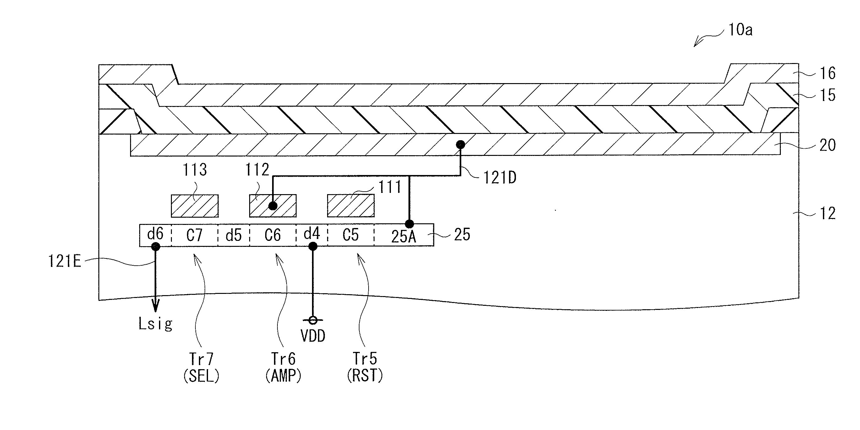
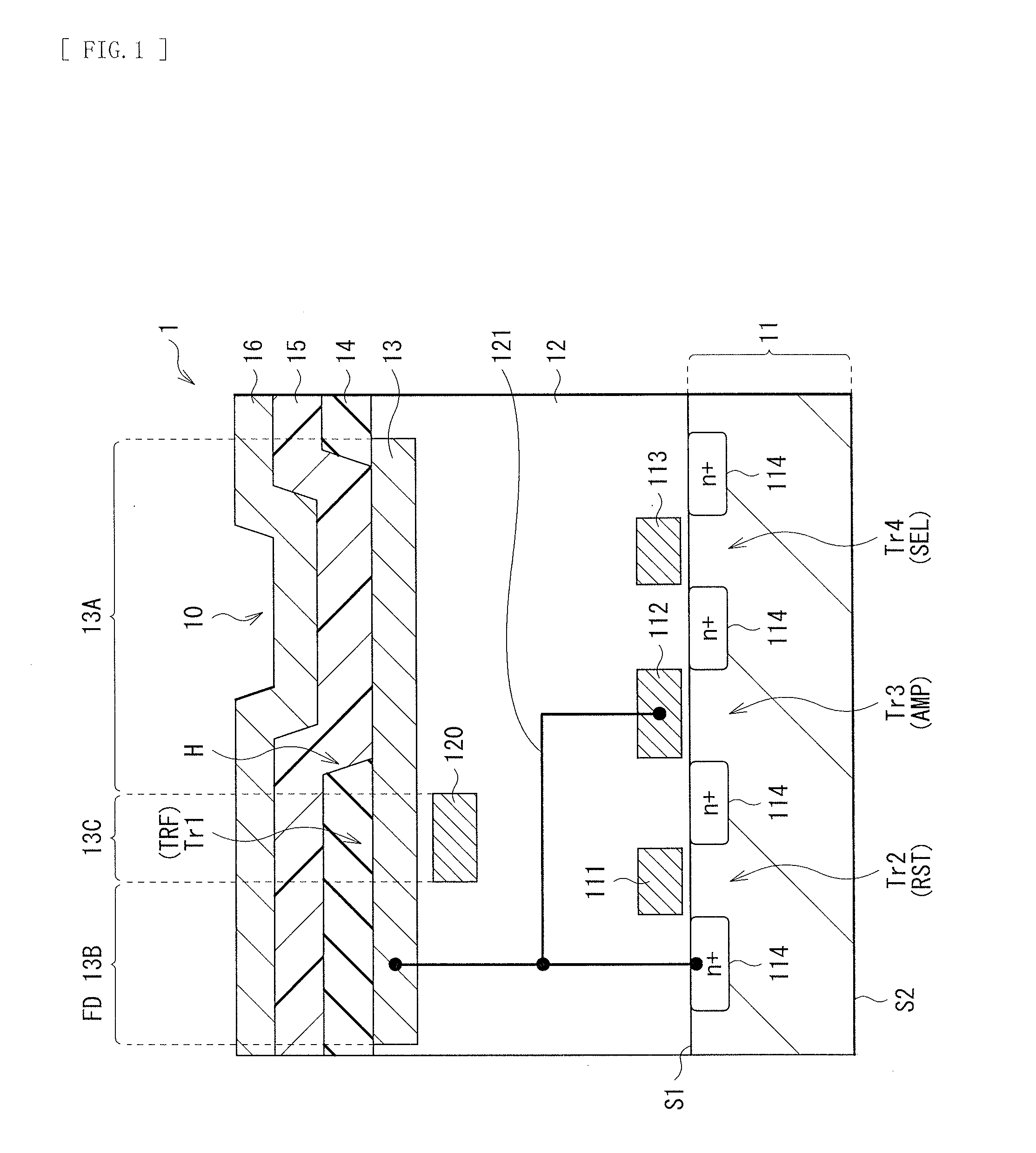
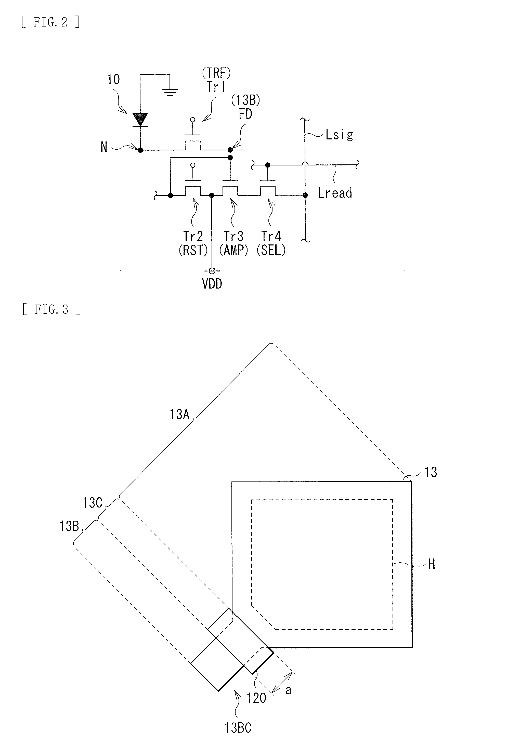
1. First Embodiment (An example of a solid-state image pickup unit (4Tr) in which a source of a transfer transistor also serves as a lower electrode of a photoelectric conversion device and a drain of the transfer transistor is connected to a gate of an amplification transistor)

2. Modification Example 1 (An example in a case where a light-shielding layer is used)

3. Modification Example 2 (An example in a case where a UV-cut filter is used)

4. Modification Example 3 (An example in a case where active layers and sources / drains of all of 4Tr are formed of a wide gap semiconductor)

second embodiment (

5. Second Embodiment (An example of a solid-state image pickup unit (3Tr) in which a gate of an amplification transistor and a source of a rest transistor made of a wide gap semiconductor are connected to a lower electrode of a photoelectric conversion device)

6. Modification Example 4 (An example in a case where a light-shielding layer is used)

7. Modification Example 5 (Another example in the case where the light-shielding layer is used)

8. Modification Example 6 (An example in a case where a UV-cut filter is used)

9. Modification Example 7 (An example in a case where active layers and sources / drains of all of 3Tr are formed of a wide gap semiconductor)

9. Application Example 1 (An entire configuration example of a solid-state image pickup unit)

application example 2 (

10. Application Example 2 (An example of an electronic apparatus (camera))


PUM


Abstract

A solid-state image pickup unit includes: a substrate made of a first semiconductor; a substrate made of a first semiconductor; a photoelectric conversion device provided on the substrate and including a first electrode, a photoelectric conversion layer, and a second electrode in order from the substrate; and a plurality of field-effect transistors configured to perform signal reading from the photoelectric conversion device. The plurality of transistors include a transfer transistor and an amplification transistor, the transfer transistor includes an active layer containing a second semiconductor with a larger band gap than that of the first semiconductor, and one terminal of a source and a drain of the transfer transistor also serves the first electrode or the second electrode of the photoelectric conversion device, and the other terminal of the transfer transistor is connected to a gate of the amplification transistor.

Description

TECHNICAL FIELD[0001]The present disclosure relates to a laminated solid-state image pickup unit including, for example, a photoelectric conversion device on a semiconductor substrate, and an electronic apparatus.BACKGROUND ART[0002]In recent years, in solid-state image pickup units such as CCDs (Charge Coupled Devices) and CMOS (Complementary Metal Oxide Semiconductor) image sensors, the number of photons entering a pixel is reduced with reduction in pixel size, and reduction in sensitivity is concerned accordingly. Therefore, a so-called laminated solid-state image pickup unit is adopted as a solid-state image pickup unit that makes it possible to achieve an improvement in sensitivity. In the laminated solid-state image pickup unit, an aperture ratio of a photoelectric conversion region is allowed to be increased by forming a photoelectric conversion layer above a semiconductor substrate made of silicon or the like.[0003]On the other hand, a longitudinal spectral solid-state image...

Claims


Application Information

Patent Timeline
Patent Type & Authority Applications(United States)
IPC IPC(8): H01L27/146H01L29/24H01L29/16H01L29/786
CPCH01L27/14612H01L29/7869H01L29/24H01L27/14645H01L29/16H01L27/14623H01L27/14621H01L27/14636H01L27/14603H01L27/14609H01L27/14665H04N25/63H04N25/70H04N25/76H04N25/134H10K39/32Y02E10/549H01L27/14643H01L27/14625H10K19/20
Inventor YAMAGUCHI, TETSUJI
Owner SONY SEMICON SOLUTIONS CORP
Why Eureka
Try Eureka