Drive device for insulated-gate semiconductor element, and power converter

a technology of insulated-gate semiconductor elements and drive devices, which is applied in the direction of power conversion systems, oscillation generators, pulse techniques, etc., can solve the problems of inability to utilize techniques, potential of hunting operations, and complicated configuration, so as to prevent thermal breakdown of insulated-gate semiconductor elements and reduce losses and noise.

Active Publication Date: 2016-01-07
FUJI ELECTRIC CO LTD
View PDF5 Cites 7 Cited by
  • Summary
  • Abstract
  • Description
  • Claims
  • Application Information

AI Technical Summary

Benefits of technology

[0026]Additionally, by supplying a constant current to the gate of each insulated-gate semiconductor element, each of the insulated-gate semiconductor elements can be turned ON without being affected by a change in ON-resistance of a semiconductor element (transistor) that drives the gate of each temperature-dependent insulated-gate semiconductor element, resulting in lowering losses and noise that occur when turning the insulated-gate semiconductor elements ON.
[0027]Therefore, based on such a simple configuration of

Problems solved by technology

Moreover, these techniques need not only to control the gate currents of the IGBTs individually in accordance with the characteristic data of the IGBTs that are obtained beforehand, but also to perform offset control on the drive control voltages and emitter voltages of the IGBTs, and these tasks are time-consuming and lead to a complicated configuration.
On the other hand, the techniques disclosed in Japanese Patent Application Publication No. 2009-159662, No. 2009-135626 and No. 2002-142492 are configured to achieve a temperature balance between two parallel-connected semiconductor elements by comparing the temperatures thereof, which means that these te

Method used


Image

  • Drive device for insulated-gate semiconductor element, and power converter
  • Drive device for insulated-gate semiconductor element, and power converter
  • Drive device for insulated-gate semiconductor element, and power converter

Examples


first embodiment

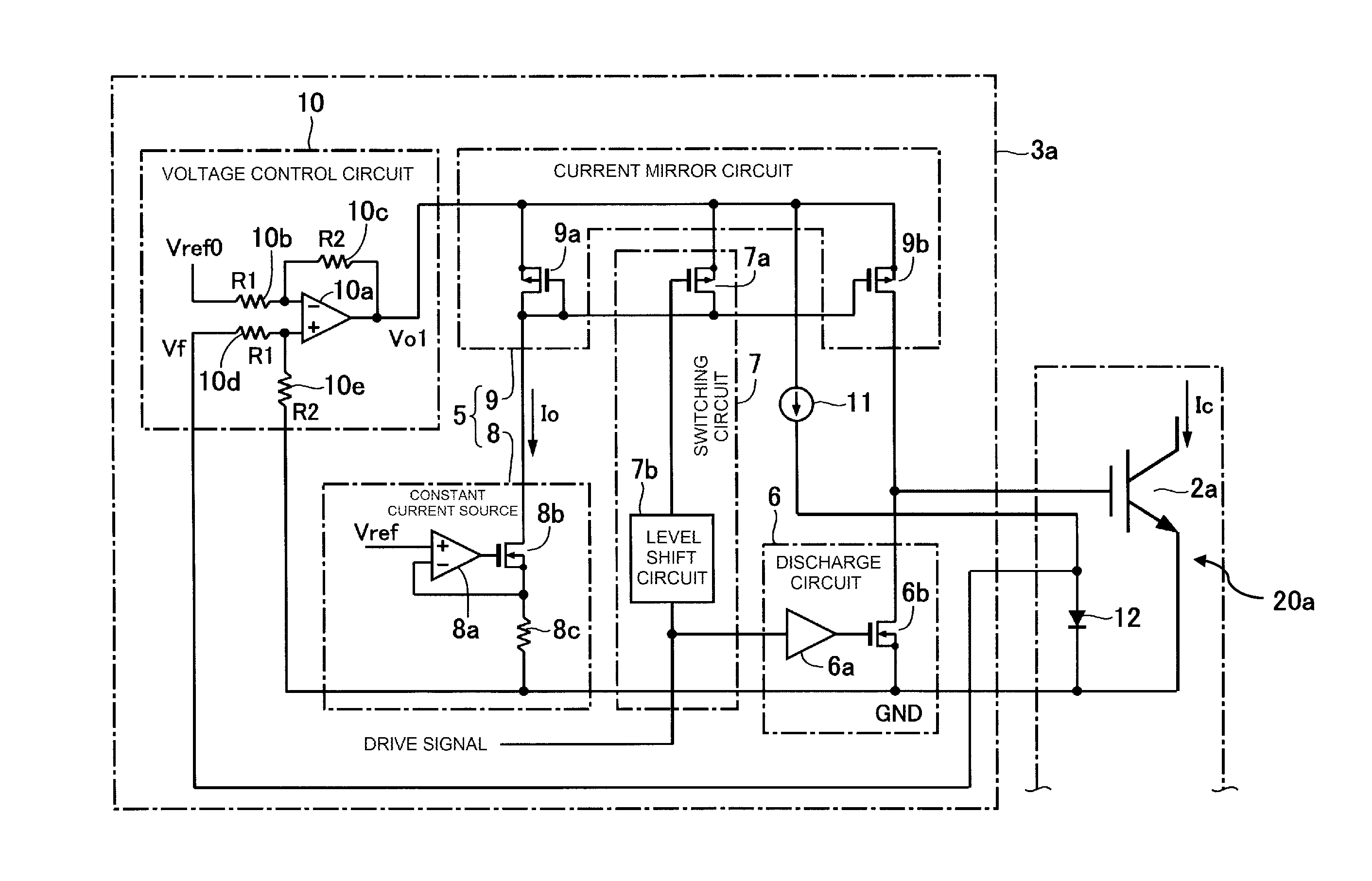
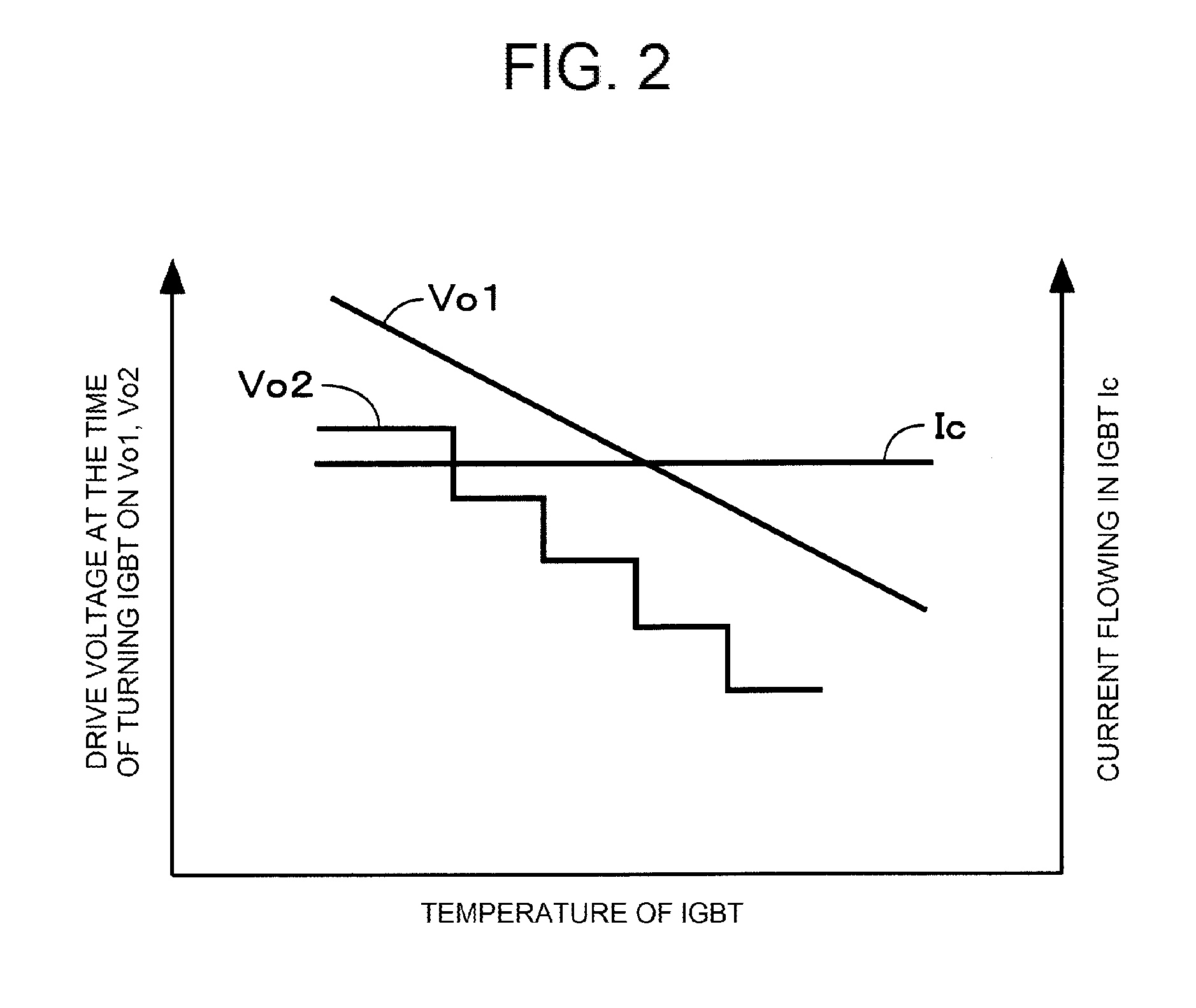
[0035]FIG. 1 is a diagram of a schematic configuration example showing substantial parts of a drive device (driver circuit) for an insulated-gate semiconductor element according to a FIG. 2 is a diagram showing turn-on drive voltage characteristics of the insulated-gate semiconductor element. Note that FIG. 1 shows a schematic configuration of a drive device 3a as a representative example, one of drive devices 3a to 3n that drive a plurality of IGBTs 2a to 2n (parallel-connected insulated-gate semiconductor elements 20) shown in FIG. 4, wherein the other drive devices 3b to 3n have the same configuration as the drive device 3a. The same reference numerals are used to describe the components same as those configuring the drive device 3a shown in FIG. 5.

[0036]The drive device 3a has a constant current source 8 and a current mirror circuit 9. The constant current source 8 and the current mirror circuit 9 configure a constant current circuit 5 shown in FIG. 5. The drive device 3a also ...

second embodiment

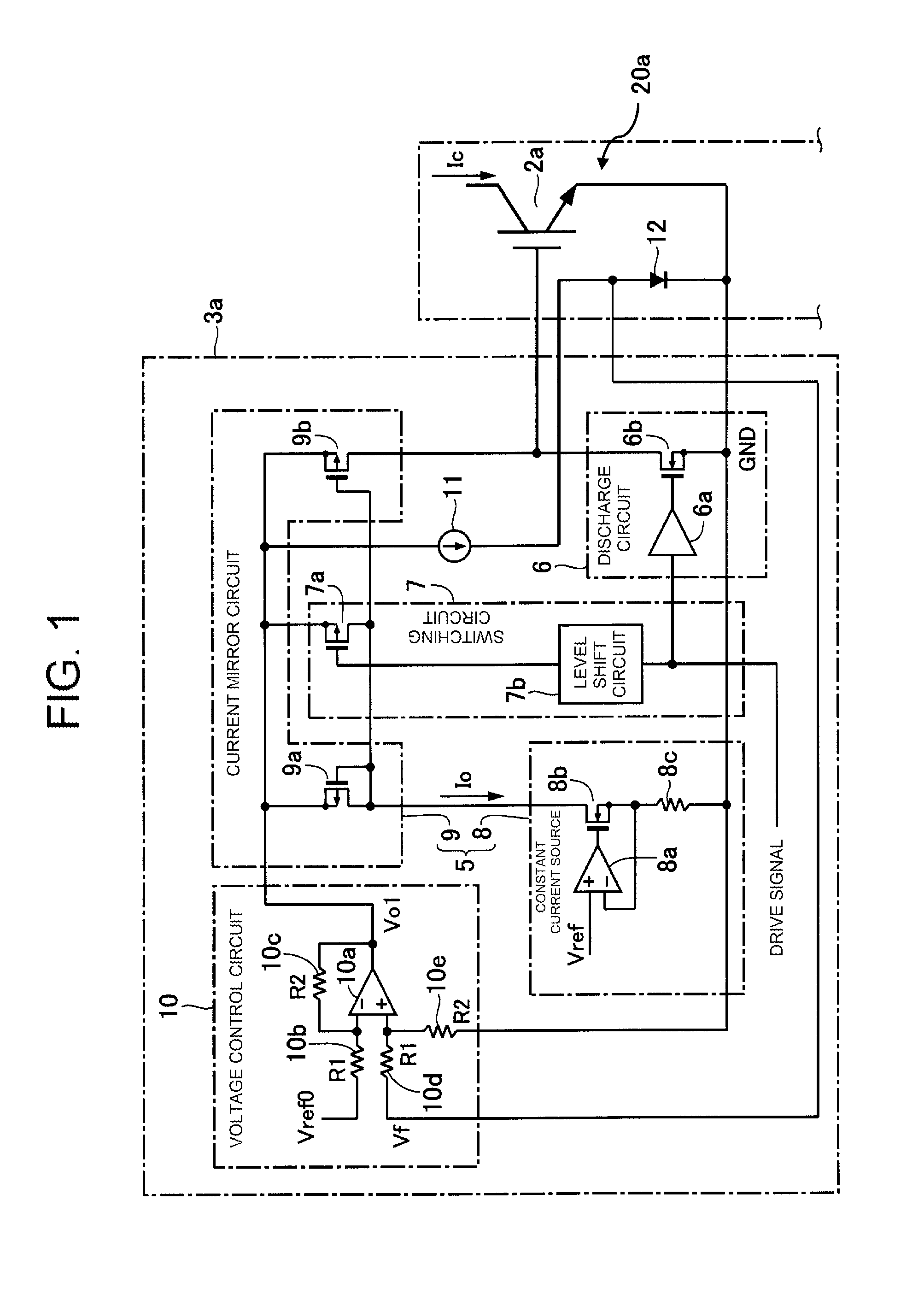
[0056]FIG. 3 is a diagram of a schematic configuration example showing substantial parts of a drive device for an insulated-gate semiconductor element according to a In FIG. 3, the same reference numerals are used to describe the components same as those shown in FIG. 1, omitting the detailed descriptions thereof.

[0057]Compared to the drive device 3a according to the first embodiment, the voltage control circuit 10 of a drive device 3a for an insulated-gate semiconductor element according to the second embodiment is replaced with a voltage control circuit 13 of a different configuration.

[0058]In other words, the voltage control circuit 13 has a plurality of (four, in the example shown in FIG. 3) comparator 13a, 13b, 13c, 13d, p-FETs 13f, 13g, 13h, 13i functioning as switch elements, and resistors 13k, 13l, 13m, 13n, 13o.

[0059]The inverted input terminals (−) of the comparators 13a, 13b, 13c, 13d are configured to receive the input of the diode voltage Vf of the temperature detecti...


PUM


Abstract

A driver circuit for turning ON and OFF one of two parallel-connected insulated-gate semiconductor elements includes a voltage control circuit that controls a level of a power supply voltage in response to a detected element temperature of the one semiconductor element, a constant current supply section, responsive to a drive signal, for supplying a constant current to a gate of the one semiconductor element to turn the one semiconductor element ON, the power supply voltage being supplied to the constant current supply section from the voltage control circuit, and a discharge circuit, responsive to the drive signal, for discharging an electric charge accumulated in the gate to turn the one semiconductor element OFF.

Description

CROSS-REFERENCE TO RELATED APPLICATION[0001]This is a continuation application of International Application number PCT / JP2014 / 064482, which was filed on May 30, 2014 and designated the United States. Furthermore, this application claims the benefit of foreign priority of Japanese application number 2013-139828, filed on Jul. 3, 2013. The disclosures of both of these earlier applications are incorporated herein by reference.BACKGROUND OF THE INVENTION[0002]1. Technical Field[0003]The present invention relates to a drive device for an insulated-gate semiconductor element and a power converter, and particularly to a drive device for an insulated-gate semiconductor element, which is capable of driving in parallel a plurality of parallel-connected insulated-gate semiconductor elements evenly with a constant current, and a power converter.[0004]2. Background Art[0005]A power converter uses IGBTs (Insulated-Gate Bipolar Transistors) for power control, MOS-FETs (Metal-Oxide-Semiconductor Fi...

Claims


Application Information

Patent Timeline
IPC IPC(8): H03K17/567H02M1/088H03K17/687
CPCH03K17/567H02M1/088H03K17/687H03K17/127H03K17/14
Inventor MORI, TAKAHIRO
Owner FUJI ELECTRIC CO LTD
Why Eureka
Try Eureka