Epitaxial graphene with thickness modulation

a graphene sheet and thickness modulation technology, applied in the direction of carbon-silicon compound conductors, magnetic recording, crystal growth process, etc., can solve the problems of insufficient flexibility of ito as electrode material, inability to meet the requirements of flexible display technology, and high cost of process for producing ito

Inactive Publication Date: 2016-01-14
SABANCI UNIVERSITY
View PDF0 Cites 5 Cited by
  • Summary
  • Abstract
  • Description
  • Claims
  • Application Information

AI Technical Summary

Benefits of technology

[0015]In the method specified above, the graphene sheet and the grid structure which is formed of graphene based ridging areas are produced integrally in situ without cumbersome extra procedures. According to a preferred embodiment, the capping structure includes protrusions that substantially limit the graphene growth on the corresponding surface of the SiC primary surface, whereas in the areas where no protrusion correspond the SiC surface grows graphene more rapidly such that ridging areas are formed. In this way, a modulated surface of graphene can be obtained on the sensitive sheet material.

Problems solved by technology

The conventional display technologies employ Indium Tin Oxide (ITO) as the electrode material which, however, is rapidly getting more expensive as the rare indium element is expected to become scarce in the near future.
In addition, ITO is not flexible enough to meet the requirements of the future flexible display technologies.
Therefore, it is the challenge for the skilled artisans in the field to obtain graphene sheets with minimum of graphene layers while ensuring maximum electronic conductivity.
Thus, it becomes an important issue to optimize the thickness of graphene sheets in order to ensure better conductivity with minimum loss in transparency.
Apparently the proposed product, especially the grid materials such as metals and carbonaceous materials have certain drawbacks as having a very low optical transparency while the process for producing the same is costly and cumbersome to practice in the real life.
However, the interface layer between SiC and graphene adversely affects the mobility of graphene grown on Si surface of SiC.
However, its growth under vacuum is fast and not self-limited, and produces high concentration of crystalline defects.
However, the state of the art techniques do not allow surface modulation of graphene sheets without excessive and exhaustive steps, and yet the need exists for straightforward methods that eliminate costly and cumbersome applications of prior art.
Moreover, it is very hard according to the conventional techniques to obtain graphene sheets having local areas with improved electrical conductivity.

Method used


Image

  • Epitaxial graphene with thickness modulation
  • Epitaxial graphene with thickness modulation
  • Epitaxial graphene with thickness modulation

Examples


example

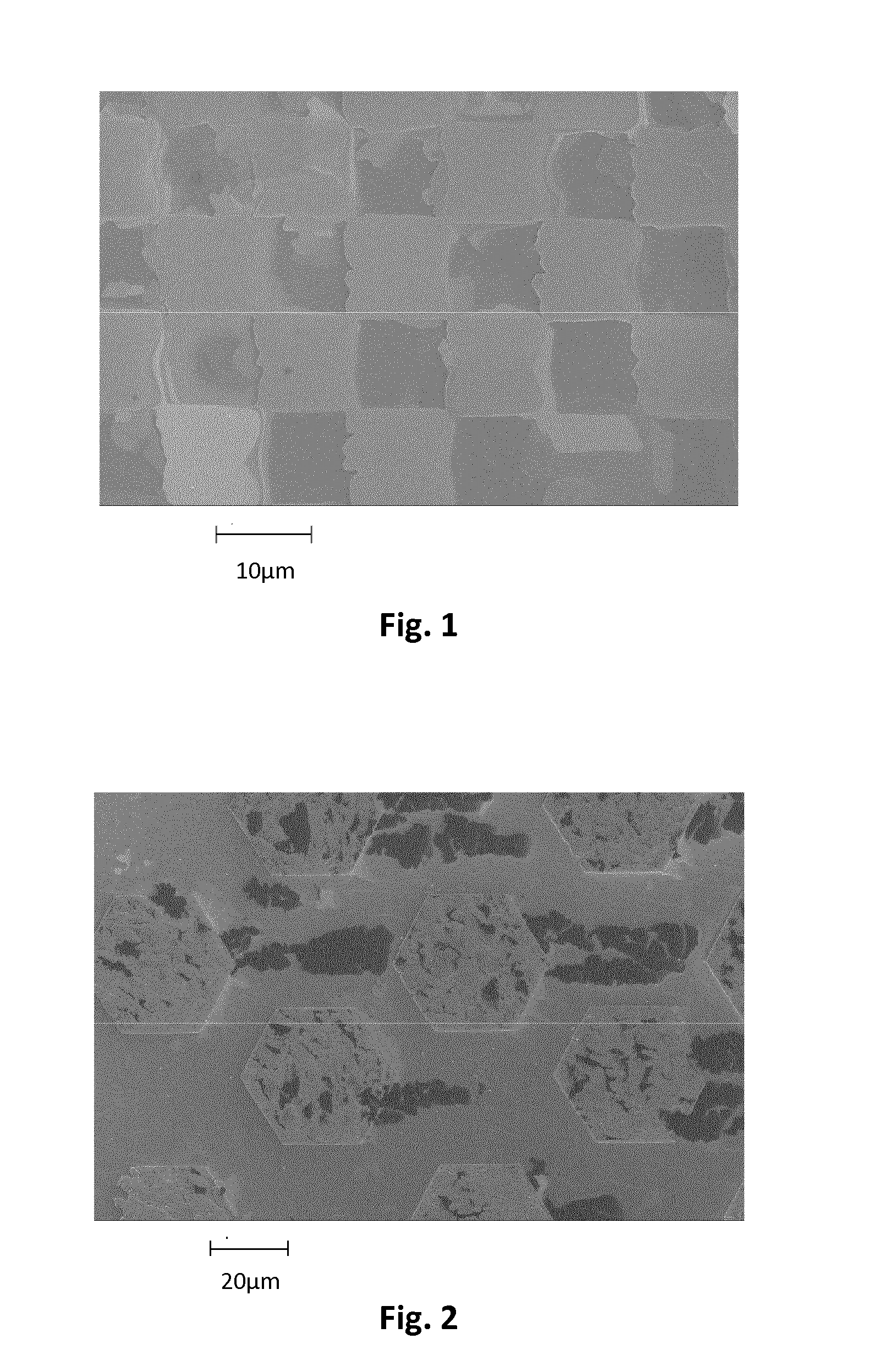
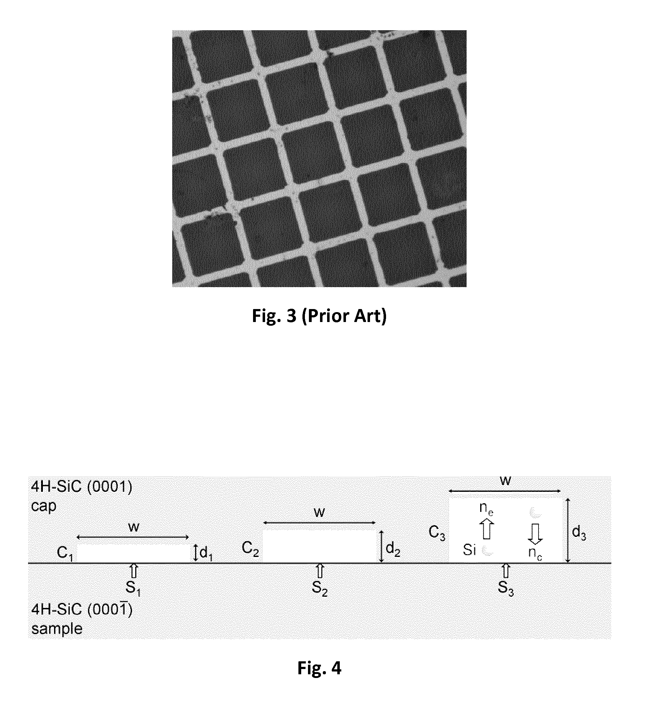
[0039]Epitaxial graphene was grown on the carbon-reach surface of SiC (000-1) substrate in ultra-high vacuum (UHV) conditions. Capping structure was also a SiC substrate. A 250 μm thick, on-axis and n-type (the doping concentration of approximately 1018 / cm3) 4H-SiC wafers with atomically flat surfaces (from NovaSiC) were used in the experiments. The wafers were diced into 3 mm wide and 10 mm long rectangular substrates and cleaned chemically. E-beam lithography, wet and dry etching processes were performed on the cap samples in order to obtain lateral height modulation with arrays of hexagonal protrusions as shown in FIG. 7a. The native oxide layers on the samples were removed in diluted HF solution prior to loading into the UHV chamber which has a base pressure of 1×10⁻¹⁰ mbar. The cap substrate was annealed in UHV by direct current heating during which the temperature is measured and controlled with 1° C. resolution individually. Cap-Sample was degassed overnight at around 600° C....


PUM

PropertyMeasurementUnit
temperatureaaaaaaaaaa
pressureaaaaaaaaaa

Abstract

The present invention relates to a novel graphene sheet with modulated thickness comprising electrically conductive areas of an array of ridges constituting a grid structure on graphene surface wherein the ridging areas are integrally formed with the graphene sheet and are themselves made of graphene. The invention further relates to a method for producing the thickness modulated graphene material of above type by way of a special capping technique where the capping structure having an array of protrusions is involved so that the said capping would transfer its physical structure to the graphene surface to form areas with improved electrically conductivity and optical transparency.

Description

TECHNICAL FIELD OF THE INVENTION[0001]The present invention relates to in situ grown graphene sheets with thickness modulation, which themselves constitute a single or multiple layers of graphene arbitrarily or regularly patterned by a given template. The invention further relates to a novel method for producing graphene sheets with grid structures in situ by way of a specially designed epitaxial growth process that is carried out in a confined and controlled atmosphere.BACKGROUND / SUMMARY OF THE INVENTION[0002]Graphene is a single layer of carbon atoms arranged in a honeycomb crystal in two dimensional structures. The realization of graphene has stimulated a large amount of experimental and theoretical research due to its extraordinary electronic and mechanical properties such as high conductance, mobility, mechanical strength, optical transparency, long spin coherence length etc. Based on these properties, graphene exhibits a very promising potential for a wide variety of new techn...

Claims


Application Information

Patent Timeline
Patent Type & Authority Applications(United States)
IPC IPC(8): C01B31/04C30B1/02C30B1/10
CPCC01B31/0461C01B2204/04C30B1/02C30B1/10B82Y30/00B82Y40/00H01B1/04C01B32/188
Inventor KAYA, ISMET INONUYANIK, CENK
Owner SABANCI UNIVERSITY
Why Eureka
Try Eureka