Methodology for annealing group iii-nitride semiconductor device structures using novel weighted cover systems

a semiconductor device and annealing method technology, applied in the direction of furnace crown/roof, heat treatment apparatus, furnaces, etc., can solve the problems of requiring specialized equipment to deal with dangerous pressures, difficult implantation activation of group iii nitride materials semiconductors, gallium nitride (gan), etc., to prevent damage to the annealing cap and sufficient flexibility

Active Publication Date: 2016-03-03
ARMY US SEC THE THE
View PDF7 Cites 8 Cited by
  • Summary
  • Abstract
  • Description
  • Claims
  • Application Information

AI Technical Summary

Benefits of technology

[0012]The protective cover may be formed of a refractory material, such as sapphire, SiC materials, Si, ZrO, MgO, YSZ, coated Si, or quartz. In some instances, the thickness of the protective cover is about 40-330 μm and the protective cover is sized larger than the surface of the capped semiconductor for which it covers. The protective cover preferably has sufficient flexibility to conform to the bow or warpage of the capped semiconductor. And to prevent damage to the annealing cap, the surface of the protective cover which faces the capped semiconductor is polished. In some embodiments, the protective cover and / or weight(s) can be a heat source of the annealing furnace. The protective cover can be advantageously provided with a ring on its top surface that is configured to hold the one or more weights, and the bottom surface of the protective cover can be provided with a rim that is configured to prevent the protective cover from sliding off the capped semiconductor.

Problems solved by technology

However, implantation activation in the Group III nitride materials semiconductors, such as gallium nitride (GaN), is more difficult than with elemental semiconductor materials.
High nitrogen over-pressure annealing can be used, but it requires specialized equipment to deal with dangerous pressures at high temperatures.

Method used


Image

  • Methodology for annealing group iii-nitride semiconductor device structures using novel weighted cover systems
  • Methodology for annealing group iii-nitride semiconductor device structures using novel weighted cover systems
  • Methodology for annealing group iii-nitride semiconductor device structures using novel weighted cover systems

Examples


Embodiment Construction

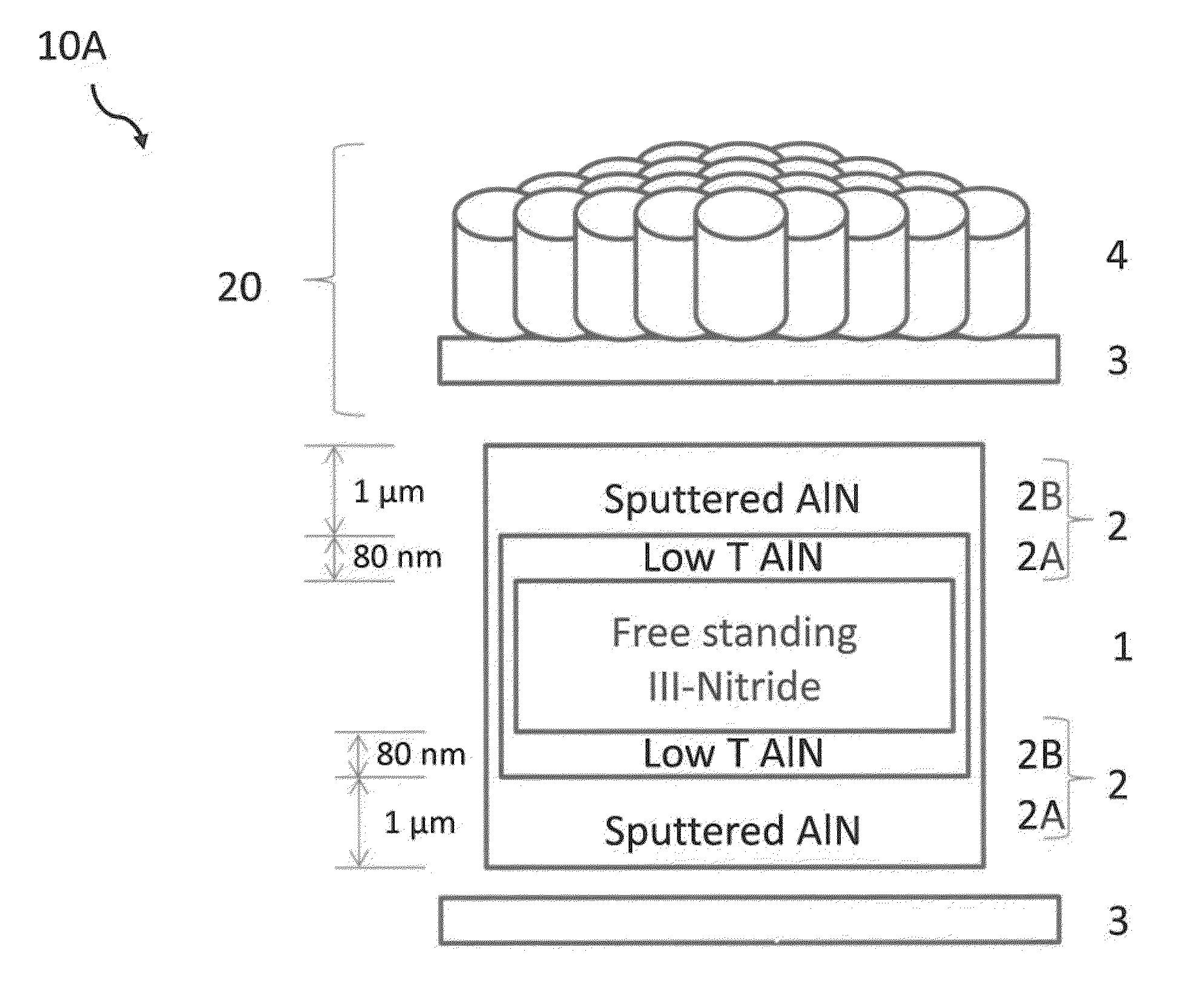
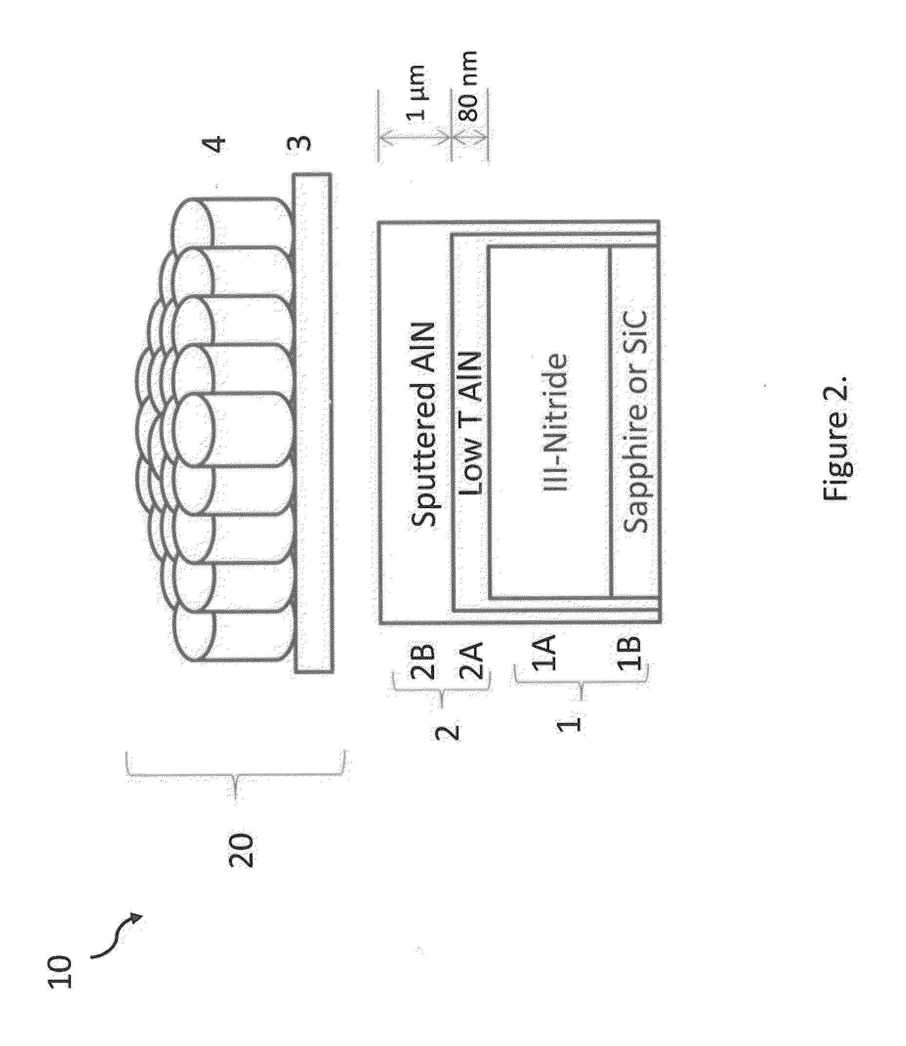
[0028]Embodiments of the present invention disclose an improved methodology for annealing group III-nitride semiconductor device structures using novel weighted cover systems that protect an annealing cap during the semiconductor annealing process.

[0029]An exemplary annealing cap structure for group III-nitride semiconductor device structures was previously disclosed in U.S. Pat. No. 7,977,224 B2, titled “Method using multiple layer annealing cap for fabricating group III-nitride semiconductor device structures and devices formed thereby,” herein incorporated by reference in its entirety. This annealing cap structure comprises a Group III-nitride semiconductor, such as gallium nitride (GaN). Formed on top of the Group III-nitride semiconductor is an annealing cap that comprises a first adherence layer and a second, thicker layer that provides mechanical strength. Both the adherence layer and the thicker layer may be formed of aluminum nitride (AlN), for instance. The first adherence...


PUM

PropertyMeasurementUnit
thicknessaaaaaaaaaa
thickaaaaaaaaaa
temperaturesaaaaaaaaaa

Abstract

An improved methodology for annealing group III-nitride semiconductor device structures using novel weighted cover systems that protect an annealing cap during the semiconductor annealing process is disclosed. The weighted cover system is configured for preventing the escape of nitrogen from the capped semiconductor during annealing. In one particular embodiment, the weighted cover system comprises a protective cover configured to be placed on the capped semiconductor during the anneal, and one or more weights configured to be placed on the protective cover to provide sufficient downward force to the protective cover that is placed on the capped semiconductor.

Description

RELATED APPLICATION DATA[0001]This application claims the benefit of U.S. provisional patent application No. 62 / 041,525 filed Aug. 25, 2014, herein incorporated by reference in its entirety for all purposes.GOVERNMENT INTEREST[0002]Governmental Interest—The invention described herein may be manufactured, used and licensed by or for the U.S. Government.FIELD OF INVENTION[0003]The present invention generally relates to semiconductor devices and semiconductor device fabrication, and in particular to, methods for activating doped semiconductor layers, materials or components by annealing.BACKGROUND OF THE INVENTION[0004]In the semiconductor industry, semiconductor wafer materials are annealed, so that dopant atoms, such as boron, phosphorus or arsenic, etc., can diffuse into substitutional positions in the crystal lattice, resulting in changes in the electrical properties of the semiconducting material.[0005]Silicon has been found to evaporate from SiC when annealed at the temperatures ...

Claims


Application Information

Patent Timeline
Patent Type & Authority Applications(United States)
IPC IPC(8): F27D1/02H01L21/324
CPCH01L21/3245F27D1/02F27B17/0025H01L21/02378H01L21/0242H01L21/0254H01L21/02667H01L21/26546C30B35/00
Inventor DERENGE, MICHAEL, A.
Owner ARMY US SEC THE THE
Why Eureka
Try Eureka