Property enhancing fillers for transparent coatings and transparent conductive films

Pending Publication Date: 2016-04-07
C3 NANO INC
View PDF9 Cites 54 Cited by
  • Summary
  • Abstract
  • Description
  • Claims
  • Application Information

AI Technical Summary

Benefits of technology

[0007]In a further aspect, the invention pertains to a transparent conductive film comprising a transparent substrate, a transparent electrically conductive layer and a protective coating comprising a polymer binder and nanoparticles. In some embodiments, the nanoparticles have an average primary particle diameter of no more than about 100 nm and are formed of a material having a bulk Vickers Hardness of at least about 1650 HV, a high thermal conductivity material selected from the group consisting of diamond, graphene, silicon nitride, boron nitride, aluminum nitride, gallium arsenide, indium phosphide or a mixture thereof and/or a high dielectric constant material selected from the group consisting of barium titanate, strontium titanate, lead titanate, lead zirconium titanate, calcium copper titanate and mixtures thereof.
[0008]In additional aspects, the invention pertains to a transparent conductive film comprising a transparent substrate and a transparent electrically conductive layer comprising a polymer binder, a sparse metal conductive element and nanoparticles. In some embodiments, the nanoparticles can have an average primary particle size of no more than about 100 nm and can be formed of a material having a bulk Vickers Hardness of at least about 1650 HV, a high thermal conductivity material selected from the group consisting of diamond, graphene, silicon nitride, boron nitride, aluminum nitride, gallium arseni

Problems solved by technology

For example, ITO is a brittle ceramic which needs to be deposited using sputtering, a fabrication process that involves high t

Method used


Image

  • Property enhancing fillers for transparent coatings and transparent conductive films
  • Property enhancing fillers for transparent coatings and transparent conductive films
  • Property enhancing fillers for transparent coatings and transparent conductive films

Examples


example 1

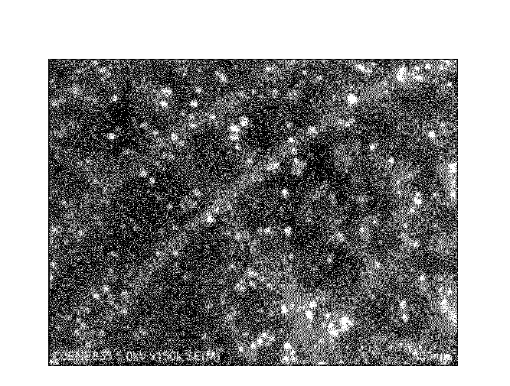
Effect of Nanodiamonds on Commercial Overcoat on a Transparent Substrate

[0098]This example tests the effect on the hardness of a commercial overcoat loaded with nanodiamonds on PET substrate with an initial polymer binder overcoat.

[0099]The substrate was prepared by coating a base ink with a cellulose based polymer binder but without any silver nanowires was coated onto a transparent PET substrate and dried. The coated substrate had a haze of 0.72%. A commercial coating polymer from Dexerials was dissolved in N,N-dimethylformamide (DMF). Six samples were prepared with two samples at each of 2 wt %, 3 wt % and 4 wt % polymer concentrations. In one sample at each polymer concentration, hydrogen terminated nanodiamonds were added, respectively, at 0.2 wt %, 0.3 wt %, or 0.4 wt % concentrations, so that in each diamond containing sample, the diamond concentrations were about one tenth the polymer concentration. The coating solutions were deposited onto the substrate by slot coating at 1...

example 2

Effect of Nanodiamond in Conductive Inks

[0100]This example tests the hardness of films having a fused metal nanostructured layers with nanodiamonds incorporated into the conductive layer with a hard coating applied over the conductive layer.

[0101]A silver nanowire ink was prepared as described above except for the addition of 0.036 wt % nanodiamonds with hydrogen terminated surface in the ink. The nanodiamonds were initially dispersed in a gamma-butyrolactone solvent prior to mixing into the silver nanowire inks. The nanowire inks were slot coated onto a PET film substrate and dried to fuse the nanowires into a fused metal nanostructured network forming a conductive layer. An overcoating composition was prepared as described in Example 1 except at a polymer concentration of 0.5 wt % and without nanodiamonds. The overcoat was processed similarly as described in Example 1 with slot coating onto the dried fused metal conductive layer, drying of the coating and UV curing the coating.

[01...

example 3

Effect of Nanodiamonds in Commercial Overcoats Over a Transparent Conductive Layer

[0103]This example tests the hardness of transparent conductive films incorporating commercial overcoats incorporating nanodiamonds.

[0104]The silver nanowire was deposited and processed as described above. Following drying, the layer comprised fused metal nanostructured network within the sparse metal conductive layer. The sheet resistances for the conductive layers were between 50 and 60 ohms / sq., and the thin overcoat layers did not significantly change the sheet resistance of the film after applying the and curing the overcoat. Two different metal nanowire ink systems were tested in combination with 3 different commercial overcoats, three different corresponding solvent systems and three different initial nanodiamond dispersions. The substrates with the fused metal nanostructured network had an initial haze prior to application of the overcoat of 1.12% with the first ink system and 1.28% with the se...


PUM

PropertyMeasurementUnit
Fractionaaaaaaaaaa
Thicknessaaaaaaaaaa
Poweraaaaaaaaaa

Abstract

Optically transparent films can comprise a coating of nanodiamonds to introduce desirable properties, such as hardness, good thermal conductivity and an increased dielectric constant. In general, transparent conductive films can be formed with desirable property enhancing nanoparticles included in a transparent conductive layer and/or in a coating layer. Property enhancing nanoparticles can be formed from materials having a large hardness parameter, a large thermal conductivity and/or a large dielectric constant. Suitable polymers are incorporated as a binder in the layers with the property enhancing nanoparticles. The coatings with property enhancing nanoparticles can be solution coated and corresponding solutions are described.

Description

CROSS REFERENCE TO RELATED APPLICATIONS[0001]This application claims priority to copending U.S. provisional patent application Ser. No. 62 / 059,376, filed Oct. 3, 2014 to Virkar et al., entitled “Property Enhancing Fillers for Coatings and Transparent Conductive Films,” incorporated herein by reference.FIELD OF THE INVENTION[0002]The invention is related to thin polymer films loaded with property enhancing nanoparticles, such as nanoparticles contributing to hardness and abrasion resistance, thermal conductivity and / or a high dielectric constant. The invention further relates to transparent conductive films incorporating a thin polymer layer loaded with property enhancing nanoparticles, which may or may not be in a layer providing the electrical conductivity and / or a coating layer associated with the transparent conductive layer. The invention also relates to transparent polymer-based films comprising nanodiamonds. In addition, the invention relates to coating solutions that comprise...

Claims


Application Information

Patent Timeline
IPC IPC(8): C09D101/02G02B1/14C09D133/14C09D163/00C09D133/08
CPCC09D101/02C09D163/00G02B1/14C09D133/14C09D133/08C08K3/04C09D101/10C09D101/18C09D101/26G02B1/16C09D7/61G02B1/04
Inventor VIRKAR, AJAYMANZOUR, FARAZ AZADIYANG, XIQIANGGU, HUA
Owner C3 NANO INC
Why Eureka
Try Eureka