Method for treating surface of silicon-carbide substrate

Active Publication Date: 2016-04-28
KWANSEI GAKUIN EDUCATIONAL FOUND
View PDF6 Cites 20 Cited by
  • Summary
  • Abstract
  • Description
  • Claims
  • Application Information

AI Technical Summary

Benefits of technology

[0029]Accordingly, a surface of a substrate has a high flatness and the

Problems solved by technology

Therefore, achievement of a semiconductor element that is able to withstand a high temperature environment is one of important problems from the viewpoint of a reliable operation, processing of a large amount of information, and improvement in the controllability in wide ranges of applications and

Method used


Image

  • Method for treating surface of silicon-carbide substrate
  • Method for treating surface of silicon-carbide substrate
  • Method for treating surface of silicon-carbide substrate

Examples


Embodiment Construction

[0049]Next, an embodiment of the present invention will be described.

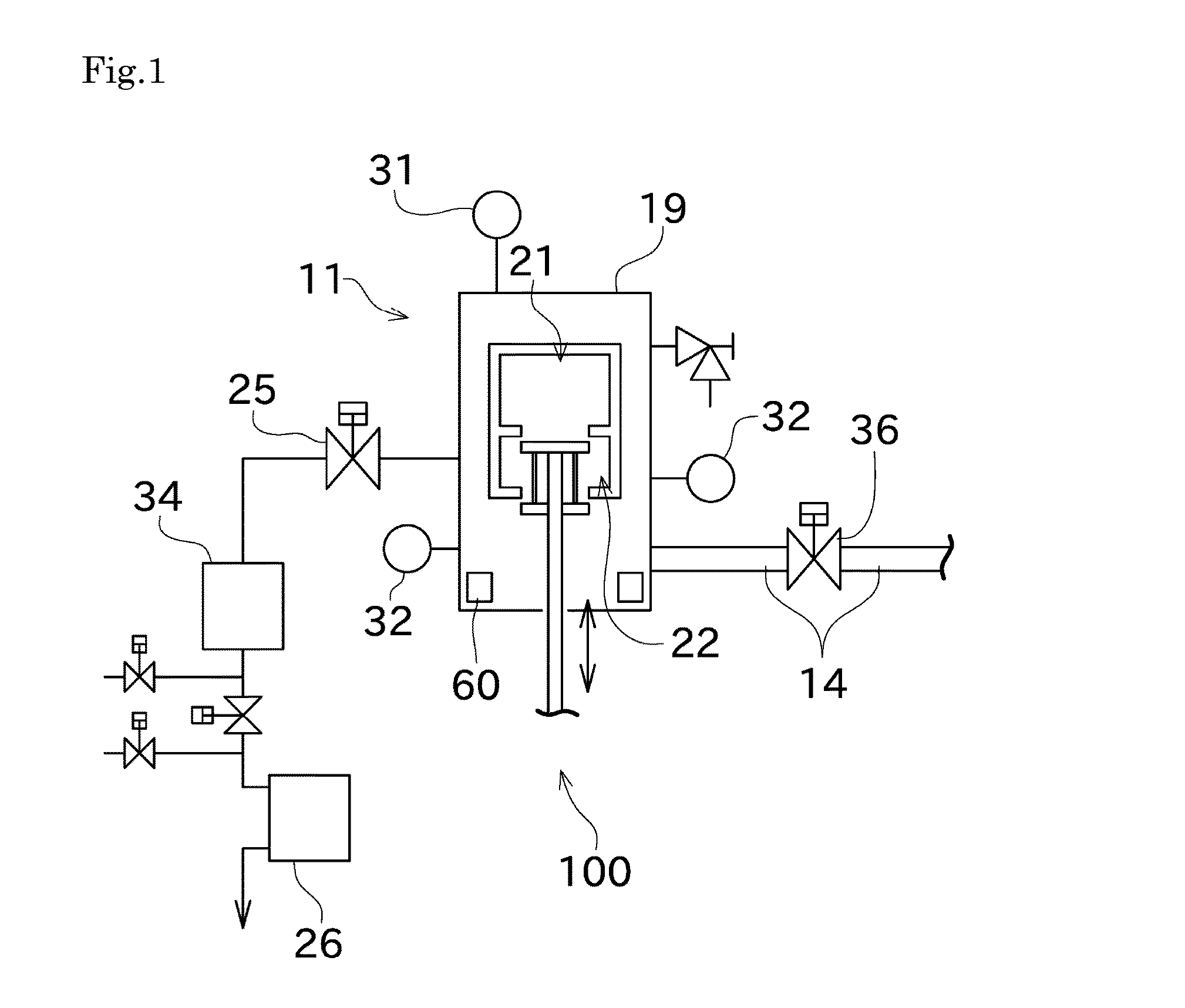
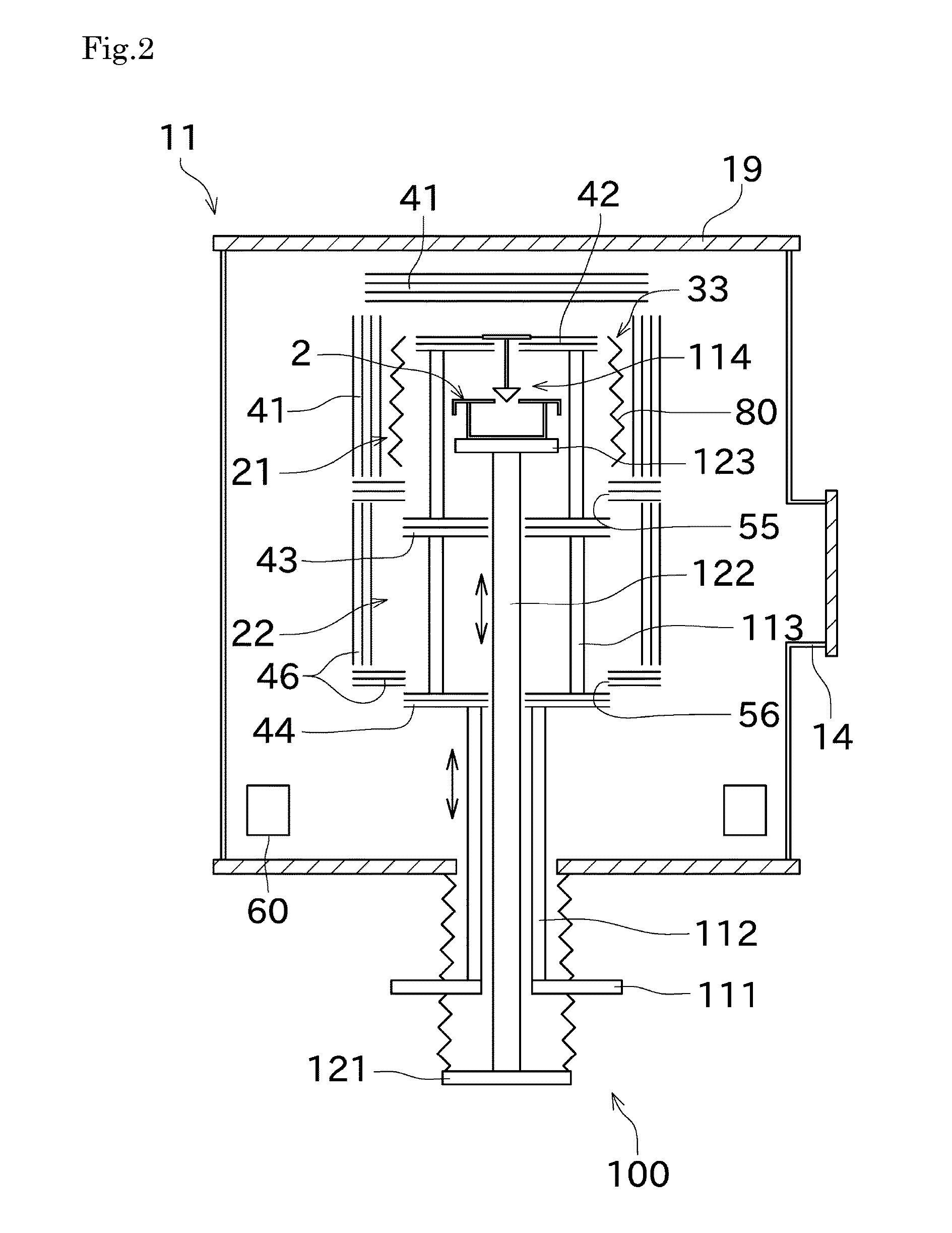
[0050]A high-temperature vacuum furnace (heating furnace) 11 and a crucible (storing container) 2 used for manufacturing a semiconductor element will be described. FIG. 1 is a schematic view showing a high-temperature vacuum furnace for use in a heat treatment for manufacturing a semiconductor element. FIG. 2 is a cross-sectional view showing mechanism details of controlling degree of sealing of a crucible in a main heating chamber of the high-temperature vacuum furnace. FIG. 3 is a cross-sectional front elevation view of the arrangement of the crucible and the like in the high-temperature vacuum furnace 11.

[0051]As shown in FIG. 1 and FIG. 2, the high-temperature vacuum furnace 11 includes a main heating chamber 21 and a preheating chamber 22. The main heating chamber 21 enables a processing object stored in a crucible 2 to be heated to a temperature of 1000° C. or more and 2300° C. or less. The preheating chamber...


PUM


Abstract

This method for treating a surface of a SiC substrate includes a first removal step in which a modified layer produced by subjecting the substrate (70) to mechanical polishing or chemical-mechanical polishing is removed by heating the substrate (70) under Si vapor pressure. A second removal step in which macro-step bunching occurred in an epitaxial layer (71) is removed by heating the substrate (70) under Si vapor pressure may also be performed. Since the etching rate can be varied, etching rate in the first removal step is high, so that the modified layer can be removed in a short time. Meanwhile, etching rate in the second removal step is comparatively low, so that excessive removal of the epitaxial layer (71) can be prevented.

Description

TECHNICAL FIELD[0001]The present invention relates to a method for treating a surface of a substrate that is made of, at least in a surface thereof, a SiC layer.BACKGROUND ART[0002]Silicon (Si), gallium arsenide (GaAs), and the like, are conventionally known as a semiconductor material. Recently, the field of use of a semiconductor element is rapidly expanding. The semiconductor element is accordingly more often used under severe environments such as a high temperature environment. Therefore, achievement of a semiconductor element that is able to withstand a high temperature environment is one of important problems from the viewpoint of a reliable operation, processing of a large amount of information, and improvement in the controllability in wide ranges of applications and environments.[0003]Silicon carbide (SiC) is of interest as one of materials that can be used for manufacturing a semiconductor element having an excellent heat resistance. SiC has an excellent mechanical strengt...

Claims


Application Information

Patent Timeline
IPC IPC(8): H01L21/04H01L21/02H01L21/306
CPCH01L21/0475H01L21/30625H01L21/02378H01L21/30604H01L21/02529H01L21/0262H01L21/02433C30B29/36C30B33/00H01L21/02658H01L21/302H01L21/3065H01L21/67069H01L21/67109H01L21/67115H01L21/68792
Inventor KANEKO, TADAAKIOHTANI, NOBORUHAGIWARA, KENTA
Owner KWANSEI GAKUIN EDUCATIONAL FOUND
Why Eureka
Try Eureka