Thin film solar cell panel and manufacturing method thereof

a solar cell and film technology, applied in the field of thin film solar cell panels, can solve the problems of difficult application of existing thin film manufacturing processes, inability to manufacture bendable photovoltaic products, and inability to manufacture solar cell components. to achieve the effect of simple manufacturing process, beautiful appearance and enhanced manufacturing efficiency

Inactive Publication Date: 2016-04-28
SHANGHAI SOLAR INVESTMENT MANAGEMENT PARTNERSHIPS S
View PDF8 Cites 8 Cited by
  • Summary
  • Abstract
  • Description
  • Claims
  • Application Information

AI Technical Summary

Benefits of technology

[0029]The manufacturing method of the thin film solar cell panel provided by the present invention has the following advantages. Every thin film layer of the thin film solar cell panel during executing the manufacturing method of the thin film solar cell panel provided by the present invention is continuous during formation thereof, and the solar cell panel is cut into smaller cell units through laser scribing only in step S3 after depositing of layers. Hence, the manufacturing process is simpler to enhance the manufacturing efficiency, and the thin film solar cell panel is able to be tightly affixed to the bending structural surface to form an integrated structure for a more beautiful appearance.
[0030]The manufacturing method...

Problems solved by technology

A glass substrate used for an existing thin film solar cell panel is too thick to have bending capacity so that the thin film solar cell panel cannot be used for making bending solar cell components.
Furthermore, it is difficult to ap...

Method used


Image

  • Thin film solar cell panel and manufacturing method thereof
  • Thin film solar cell panel and manufacturing method thereof
  • Thin film solar cell panel and manufacturing method thereof

Examples


Embodiment Construction

[0050]The present invention will be described in detail in conjunction with preferred embodiments shown in the accompany drawings as follows. However, these described embodiments are not provided to limit the present invention. All variations of structures, methods or functions made by a person of ordinary skill in the art according to these embodiments are covered within the protection claim scope of the present invention.

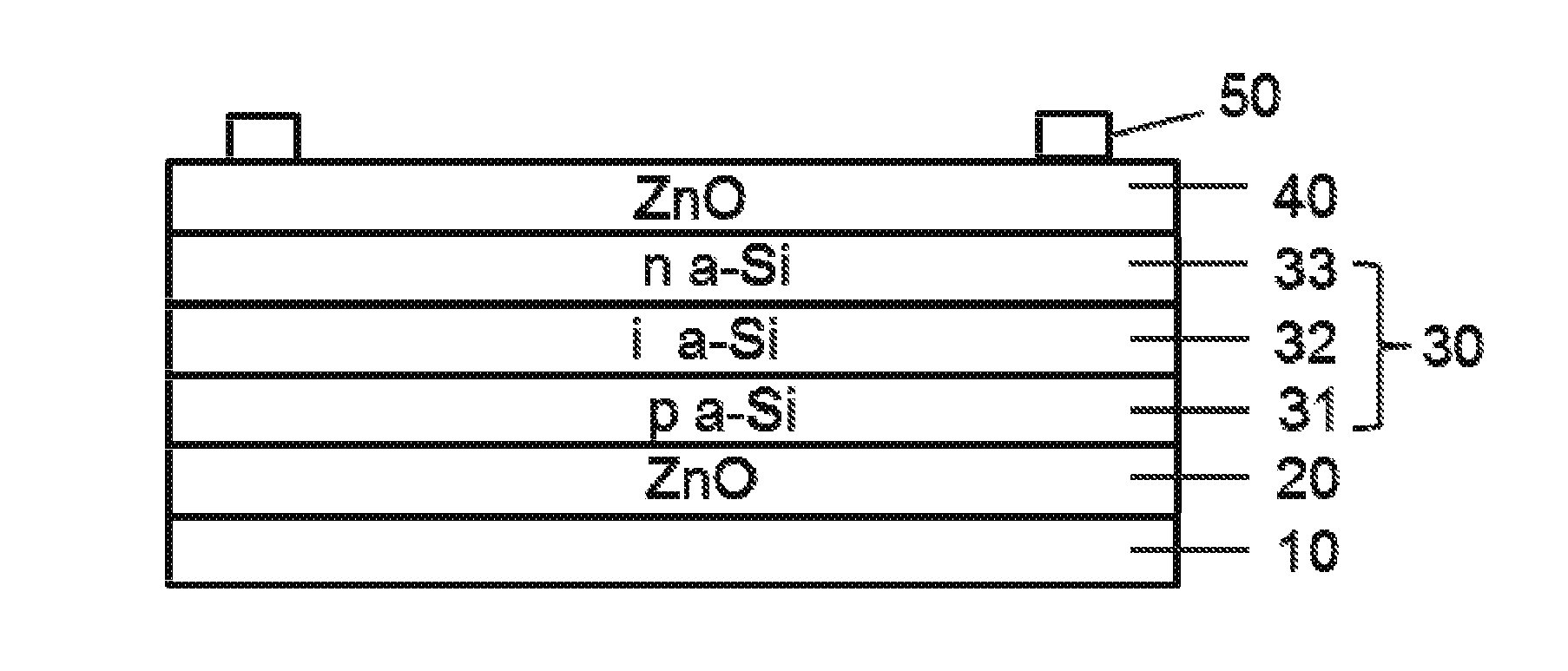
[0051]FIG. 1 is a schematic structural diagram of a thin film solar cell panel in accordance with a preferred embodiment of the present invention. With reference to FIG. 1, the thin film solar cell panel includes a substrate 10, a first electrode 20 disposed on the substrate 10, a photoelectric conversion layer 30 disposed on the first electrode 20, a second electrode 40 disposed on the photoelectric conversion layer 30 and a gate electrode 50 disposed on the second electrode 40. The substrate 10 is an ultra-thin glass substrate. A thickness of the ultra-thin glas...


PUM


Abstract

The present invention provides a thin film solar cell panel and a manufacturing method thereof. The thin film solar cell panel comprises a substrate, a first electrode disposed on the substrate. The substrate is an ultra-thin glass substrate with a thickness of 0.1-1 mm. The ultra-thin glass substrate has a bending capacity, and a minimum bending radius thereof reaches below 10 cm. The first electrode is continuously disposed on the substrate during its formation. Light transmittance of the thin film solar cell panel of the present invention is enhanced, and the thin film solar cell panel can be conveniently used to manufacture a bending solar cell component.

Description

FIELD OF THE INVENTION[0001]The present invention relates to the field of solar photovoltaic products, and particularly to a thin film solar cell panel and a manufacturing method thereof.BACKGROUND OF THE INVENTION[0002]A thin film solar cell has experienced a long development process from its invention to mass commercialization. In 1976, the first amorphous silicon thin film solar cell was successfully developed by Radio Corporation of America (RCA). After entering the mid 90s of the last century, with continuous progress of semiconductor manufacturing equipment and manufacturing technology, a highly efficient laminated silicon-based thin film solar cell is made to achieve large-scale commercial production, and optical absorption material of the silicon-based thin film solar cell was developed from an original homogeneous structure of amorphous silicon to a heterogeneous structure composed of amorphous silicon, polycrystalline silicon and monocrystalline silicon. In addition to the...

Claims


Application Information

Patent Timeline
IPC IPC(8): H01L31/0468H01L31/18B60J7/043H01L31/0463H01L31/0445
CPCH01L31/0468B60J7/043H01L31/1876H01L31/0463H01L31/03921H01L31/03926H01L31/0445Y02B10/10Y02E10/548H01L31/022425H01L31/022466H01L31/18H02S10/40H02S20/26Y02E10/50
Inventor YANG, LIYOUWANG, HAO
Owner SHANGHAI SOLAR INVESTMENT MANAGEMENT PARTNERSHIPS S
Why Eureka
Try Eureka