

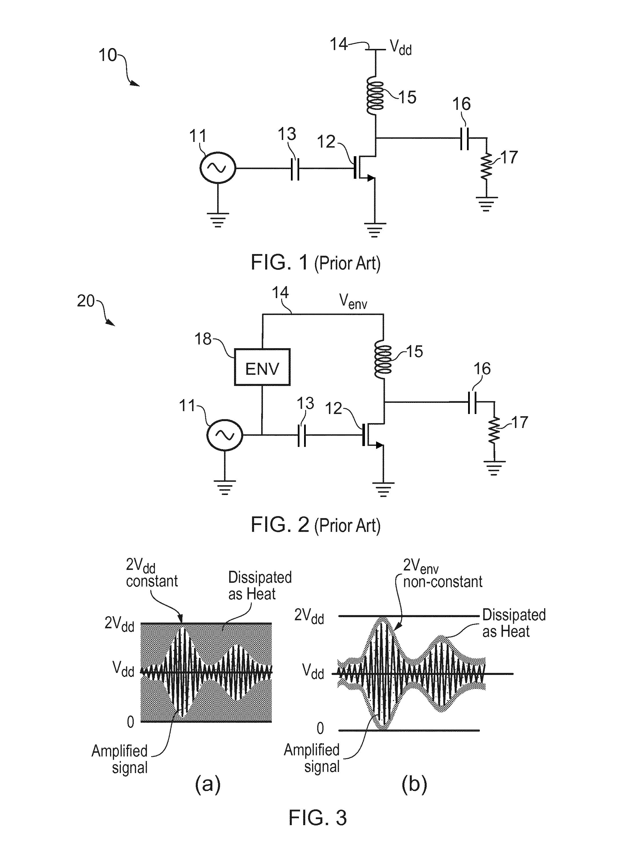
Amplifier Topology for Envelope Tracking
- Summary
- Abstract
- Description
- Claims
- Application Information
AI Technical Summary
Benefits of technology
Problems solved by technology
Method used
Image

Examples
first embodiment
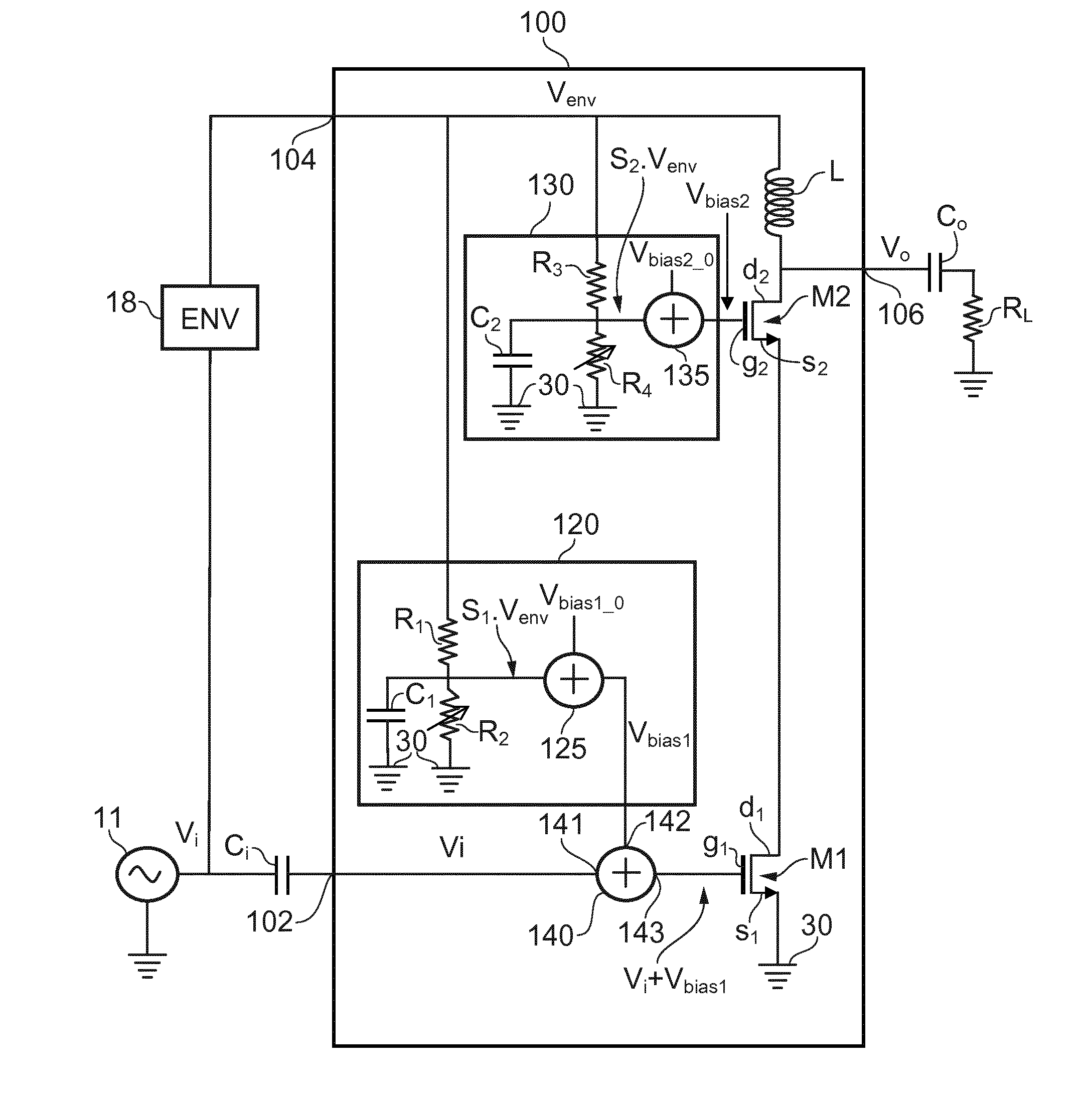
[0039]FIG. 6 is an amplifier in accordance with the present disclosure;
[0040]FIG. 7 illustrates load lines for different values of the envelope signal;
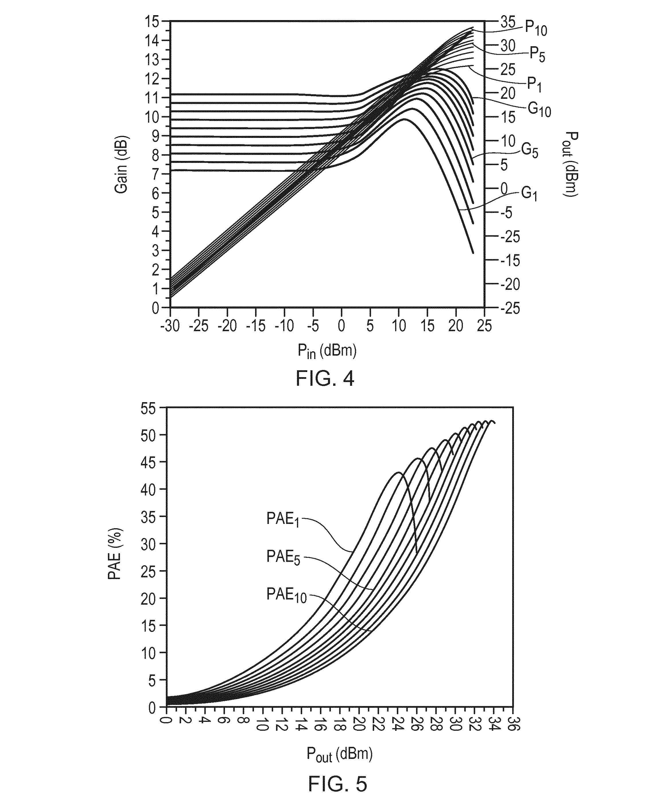
[0041]FIG. 8 is a graph of gain and output power as a function of input power for an amplifier with tracking bias voltages in accordance with the present disclosure;
[0042]FIG. 9 is a graph of gain and output power as a function of input power without tracking bias voltages;
[0043]FIG. 10 is a graph of current as a function of output power;
[0044]FIG. 11 is a Smith chart illustrating input impedance;
[0045]FIG. 12 is a graph of Rollet stability factor;
[0046]FIG. 13 is a graph of small signal gain as a function of frequency;
[0047]FIG. 14 is a flow chart of a method of amplification;
[0048]FIG. 15 is a flow chart of a method of calibrating an amplifier;
second embodiment
[0049]FIG. 16 is an amplifier in accordance with the present disclosure; and
[0050]FIG. 17 is a block schematic diagram of an electronic apparatus comprising an amplifier.
PUM
 Abstract
Description
Claims
Application Information